Indian Electronics and Semiconductor manufacturing industry

notaname

Senior Member
Joined
Dec 11, 2020
Messages
3,057
Likes
16,021
Country flag
Govt is dillydalling. According to Arun Mamphazy Govt has 12 proposals already instead of approving them. They are coming up with a new plan. They want the big shots like TSMC and Samsung. They are too big a fish for us right now.
It's good if they are batting on every option we only have one shot at this if we miss this we will not have another opportunity for years either we do it right or loose the opportunity altogether and those companies applied are not going anywhere they are there for perks they will wait just they are anxious they may lose if bigger players come in picture and we need bigger players to have significant workforce trained.
 

Ajax01

Regular Member
Joined
Feb 29, 2020
Messages
360
Likes
1,183
Country flag
Just catchup won't work. Research must be funded for CNT 3D chips. We need to disrupt other countries as well and become the leaders.
 

warriorextreme

Senior Member
Joined
Sep 29, 2010
Messages
1,870
Likes
3,050
Country flag

Sharda Motor and Kinetic Green form JV company for Lithium‐ion Battery packs manufacturing

Sharda Motor Industries Limited (SMIL) and Kinetic Green Energy & Power Solutions Limited, a Kinetic Group company, have entered a joint venture (JV) agreement, to develop Battery Packs with Battery Management Systems (BMS) for electric Vehicles & stationery applications.

The JV company will undertake the design, development & assembly of lithium‐ion battery packs along with BMS. The focus of the company will be to develop battery packs for the rapidly growing electric vehicle market in India & other segments of energy storage applications.

According to the regulatory filing, the company has inked a technical collaboration with the Indian Institute of Technology, Madras, India’s premier academic and research institution in India for the same. Under the technical collaboration agreement, the Centre for Battery Engineering and Electric Vehicle (CBEEV), the research and development centre of IIT Madras, will provide technology for Li‐ion battery energy storage for electric 2 wheelers, 3 wheelers and other small electric vehicles to the JV.

The technology developed at IIT Madras includes advanced thermal design to overcome adverse temperatures in India, mechanical designs to overcome vibrations due to varying road conditions, as well a Battery Management System designed by CBEEV IITM keeping in mind Indian road conditions.
 

warriorextreme

Senior Member
Joined
Sep 29, 2010
Messages
1,870
Likes
3,050
Country flag

Electronics firms Foxconn, Flex, Jabil, Sanmina among 29 register under telecom PLI scheme

Global electronics manufacturing companies Foxconn, Flex, Jabil Circuit, Sanmina SCI are among 29 companies that have registered under the Rs 12,195 crore production linked incentive scheme for the telecom sector, according to an official source.

Another source said that Foxconn and its subsidiary Rising Stars Mobile have registered for the scheme separately with the project management agency of the scheme, Small Industries Development Bank of India (SIDBI).

"Telecom PLI is seeing interest from all global major investors. Foxconn, Flex, Jabil Circuits, Sanmina SCI, Nokia and several companies have registered for it. Total 29 companies have registered for it till Wednesday. There is still about a week left for the deadline. We expect more companies to come," an official source told PTI.
 

warriorextreme

Senior Member
Joined
Sep 29, 2010
Messages
1,870
Likes
3,050
Country flag

‘World’s cheapest wafer’ maker plans 2 GW Indian cell and wafer fab

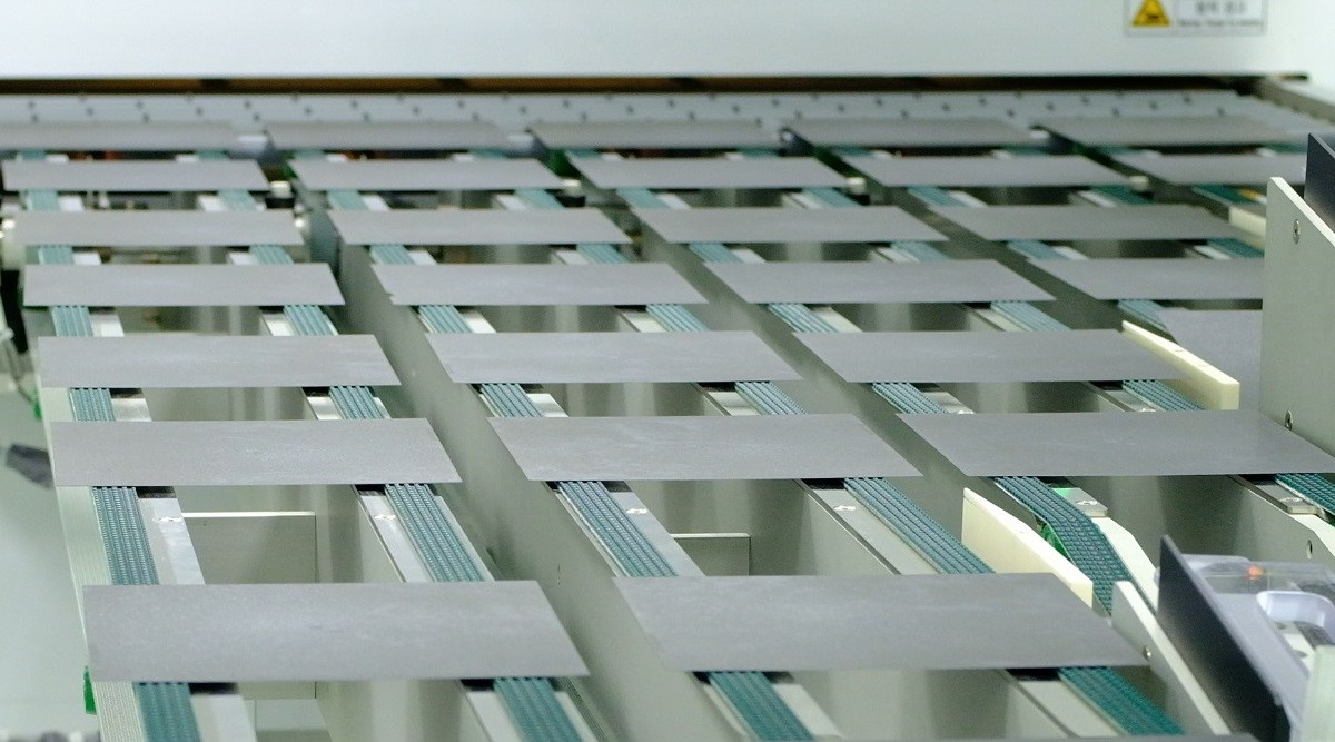
U.S. business 1366 Technologies is looking for Indian module manufacturing partners as it plans to bring its ‘direct wafer’ production technique to the country. The company uses molten silicon to form wafers rather than sawing ingots, thus eliminating dust waste and speeding up the process.

U.S.-based wafer manufacturer 1366 Technologies has confirmed plans for a 2 GW wafer and cell production facility in India. The unit is being planned under the Indian government’s production-linked incentive (PLI) scheme, which aims to drive deployment of every stage of the solar supply chain, from polysilicon to module manufacturing.

A spokesperson for the company told pv magazine it is exploring manufacturing opportunities for its ‘direct wafer' production process in India and the business said it is also seeking solar module partners.

“The Indian government has made domestic solar manufacturing a priority and our technology is particularly well suited for the Indian market,” said the 1366 spokesperson. “Direct wafer manufacturing can immediately deliver the lowest cost of electricity in a single-junction device for India’s utility market, and it underpins an economically feasible, high-efficiency, tandem product for global leadership.”

Kerfless
The direct wafer process is a kerfless wafer technique, meaning it does not require silicon ingots to be sawn into wafers, a time-consuming process that wastes material as silicon dust. Instead, 1366’s technology forms wafers directly, using molten silicon.
The company claims its direct wafer process offers the world’s lowest wafer production cost, translating into cell and module competitiveness.

The direct wafer approach has long held big hopes for the industry and the company operates a demonstration facility in Bedford, Massachusetts, where most of its technological developments were achieved. One such was a 20.3% cell efficiency level recorded in August 2017 in a Q Cells Q.antum cell which incorporated passivated emitter rear contact (PERC) technology and 1366 wafers. That record, 1366 Tech said at the time, was achieved on a pilot line using standard processes seen in mass production.
 

warriorextreme

Senior Member
Joined
Sep 29, 2010
Messages
1,870
Likes
3,050
Country flag

Haldilal

लड़ते लड़ते जीना है, लड़ते लड़ते मरना है
Senior Member
Joined
Aug 10, 2020
Messages
29,625
Likes
113,908
Country flag
ASML's production queue must have been booked for years to come. All the best to us for getting machines from them in this decade.
Ya'll Nibbiars second hand 90 NM like machine like the Changirah facility 180 NM machines which were brought from the Tower Tazz has to start from somewhere. Can't directly jump to the 7 NM. Or else can order the Equipment from the Japanese. They are not as advance as the ASML or below 22 NM but can be useful to setup the initial Chip industries.
 

FalconSlayers

धर्मो रक्षति रक्षितः
Senior Member
Joined
Oct 14, 2020
Messages
27,912
Likes
193,270
Country flag


Haldilal

लड़ते लड़ते जीना है, लड़ते लड़ते मरना है
Senior Member
Joined
Aug 10, 2020
Messages
29,625
Likes
113,908
Country flag
Ya'll Nibbiars the Samsung and the TSMC is developing the Next Generation Lithography Machines don't knew when it will happen but will break the ASML Dominance.

ASML scanner cost around 120 million Us dollar's. And uses the AGC and Hoya Blank photomasks. A typical EUV tool weighs 180 tons.

600px-Extreme_ultraviolet_lithography_tool.jpg
 
Last edited:

aragonishere

Regular Member
Joined
Oct 28, 2017
Messages
50
Likes
189
Country flag
India can become leading chip manufacturer if China ban prevails for then 3 years and PLI gets key chip manufacturers to start production.
 

omaebakabaka

Senior Member
Joined
Aug 29, 2020
Messages
4,945
Likes
13,835
Ya'll Nibbiars 150 million dollar machine.

View attachment 98405
It is always better to take the lead on the cusp on these things which means promote and patronize more practical research that is upcoming and build prototypes....this is how you catch up. Kind of pointless to recreate and try to reach the incumbents accomplishments....ofcourse we need to buy whatever for immediate purpose
 

Haldilal

लड़ते लड़ते जीना है, लड़ते लड़ते मरना है
Senior Member
Joined
Aug 10, 2020
Messages
29,625
Likes
113,908
Country flag
Ya'll Nibbiars 150 million dollar machine.

View attachment 98405
Ya'll Nibbiars this one actually cost 178 million Us Dollar's. And to produce 30,000 wafers annually 24 Hours, 365 days will need atleast one. The whole process requires Three months to produce one wafer from start to finish. You have four harvest.
 
Last edited:

Cheetah007

Regular Member
Joined
Jun 17, 2020
Messages
191
Likes
687
Country flag
Here is Professor Anantha's profile

He has more than 100,000 Google scholar citations. He is doing a fantastic job by sending students to IIT for research collaboration. He works on the semi conductors and advanced detectors.

Word of mouth is that " It's not if he will get the Nobel laureate, it's when he will get it"

People like them are already inspiring the youth of India.
 

Haldilal

लड़ते लड़ते जीना है, लड़ते लड़ते मरना है
Senior Member
Joined
Aug 10, 2020
Messages
29,625
Likes
113,908
Country flag
Ya'll Nibbiars this is one of the possible setup for 40 to 90 NM Wafer productions.

images - 2021-07-06T102702.654.jpeg
 

Indx TechStyle

Kitty mod
Mod
Joined
Apr 29, 2015
Messages
18,357
Likes
56,611
Country flag
PRC is about to get its own lithography machine (28 nm) quite soon. I'm wondering whether there's even a proposal in India to try building a litho.
 

Latest Replies

Global Defence

New threads

Articles

Top