BHARAT’s Semiconductor Research Efforts

asaffronladoftherisingsun

Dharma Dispatcher
New Member
Joined
Nov 10, 2020
Messages
12,207
Likes
73,694
Country flag
This article looks at BHARAT’s ongoing micro-controller & micro-processor R&D work in defence, space, telecom, IoT and other strategic sectors. Most of this R&D is funded by DRDO, MeitY, ISRO and related agencies (under direct/indirect control of the Government of India). While this has been the case so far, in recent years participation from academia & the private sector has increased substantially.

The need for Indian micro-controllers & micro-processors

In the early years, the need for micro-processors & micro-controllers was driven exclusively by the defence & space sectors. India’s 1st orbital launch vehicle was Indian Space Research Organisations’s (ISRO) Satellite Launch Vehicle (SLV) which was developed in the 1970s. In the early 1980s, the project director of the SLV program, Dr. APJ Abdul Kalam, was inducted into the Defence Research and Development Laboratory (DRDL) for the development of various guided missiles for the military.

The project was named the Integrated Guided Missile Development Program (IGDMP). From ballistic missiles to SAMs to ATGMs, IGDMP was an umbrella program for all kinds of guided missiles.

Understandably, India’s initial line up of guided missiles & launch vehicles used RF controlled solenoid driven actuation systems. As missile tech matured in the country demand for micro-controllers for actuation & micro-processors for On-Board Computers (OBCs) grew. Today, processors are increasingly common in a guided missiles & launch vehicles.

Thus design, fabrication, raw materials & component sourcing is becoming increasingly important to national security.

Differences between micro-controllers & micro-processors
A micro-controller is a very small, low-cost microcomputer designed to perform a specific task. These tasks could be displaying information, receiving remote signals, rotating the actuation motor to a particular angle etc.

The above table highlights the differences between a microprocessor and a microcontroller.[1]

The general micro-controller consists of the micro-processor, the memory (RAM, ROM, EPROM), Serial ports, peripherals (timers, counters), etc. All these systems are packaged into a single unit.[1]

In most missiles, a single powerful micro-processor is used along with a number of micro-controllers. The sensors on the missile sends data to the micro-processor which decides the action to be performed according to the mission requirement. The command from the micro-processor travels to the micro-controllers which manipulate the control surfaces/nozzle/TVCs to change/maintain course as needed.

Typically the motherboard containing the micro-processor & the daughter boards with the micro-controllers are stacked together to form what is known as the On-Board Computer (OBC). This stacking is done to minimize space taken up by the electronics inside a missile.
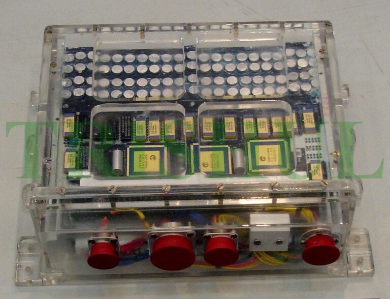
Missile-Interface-Unit-768x588.jpg


Missile Interface Unit of the Nirbhay missile.[2]


View attachment 132939


On-Board Computer of then Nirbhay missile. A processor from Intel is visible.[2]


Path of indigenisation for micro-controllers & micro-processors
The semi-conductor business is a critical & expensive business. The investments needed to have a foundry with state-of the art technology is in the range of hundreds of billions of US$. For a developing country like India setting up a foundry with the latest tech is not feasible.

Hence, the path chosen by the GoI to indigenise semi-conductors is as follows:

  1. Import generic processors from Intel et al and build systems around them. Acquire experience in system design, coding, algorithms etc.
  2. Acquire expertise in simple & eventually complex VLSI chip designs. Have them fabricated abroad. Build systems around those custom built chips.
  3. Set up some fabrication ability in the country. Nothing very expensive. But good enough to make most low-mid capacity chips that are needed in quantity.
  4. Once sufficient skills have been acquired in ship fabrication, move up the ladder. Upgrade the production facilities for both better technology node & production capacity.
Currently we are in step 3. Most our current weapon systems use a combination of American & Indian micro-processors. We continue to use them as Intel Corp. continues to pump out generic chips by the millions. That makes them price competitive as domestic chip making hasn’t still acquired such scale. Besides New Delhi doesn’t have any major problems with Washington, yet.

Indian efforts in semiconductors
Defence

DRDO has set up the Society for Integrated Circuit Technology & Applied Research (SITAR) & Advanced Numerical Research & Analysis Group (ANURAG) to design systems required for many DRDO projects. ANURAG was set up in the 1980s & SITAR in 2003. Prior to 2003, SITAR was a part of ITI Ltd. & played a lead role in development of ASIC for telecommunications in India.

They have 3 fabrication & packaging units :

  1. Semiconductor Technology & Applied Research Centre (STARC) at Bangalore. A majority of the critical RF, MEMS sensors & some micro-controllers are made in this facility.
  2. Gallium Arsenide Enabling Technology Centre (GAETEC) at Hyderabad. Most of the micro-processors & micro-controllers used in military communication equipment and the OBCs of Indian aircrafts, missiles & munitions are made by GAETEC.
  3. A smaller prototyping fab at SITAR probably using a 100 nm CMOS technology.[10]
In the early days, SITAR & ANURAG used to design chips & get them manufactured abroad. But since the early 2010s, the facilities have seen major up-gradation. This has led to a drastic reduction in the need for contract manufacturing from abroad.

DRDO states that the STARC facility is a 1 micron digital CMOS, DLM and MIL qualified fab with capability to process 150 mm wafers. MEMS fabrication facility also was established in 2012. MEMS Packaging & Testing Facility have been added in 2017.

GAETEC, on the other hand, started off by absorbing the process technology developed at DRDO’s Solid State Physics Laboratory (SSPL) & has been producing MMICs with 0.7 micron gate length MESFETs (G7a) and 0.5 micron gate length MESFETs (G5A) in GaAs Fab.

SSPL focused on standardizing semi-conductor production method, equipment & tooling to help GAETEC scale up manufacturing. Somewhere along the way they stopped investing in their Metal-Semiconductor Field Effect Transistor (MESFET) technology & went with the Standard Cell technology.

More recently a project entitled AlGaN/GaN High Electron Mobility Transistors: Material and Device Technology Development (BALRAM) was undertaken by Solid State Physics Laboratory (SSPL). Under this project SSPL developed & standardized production practices for GaN HEMTs for their use in the military & space sectors.
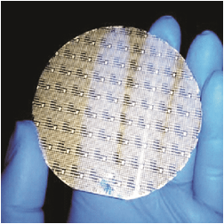
a1.png


AlGaN/GaN HEMT processed wafer from the SSPL facility. Photo Credit: SSPL, DRDO.

SSPL currently serves as the primary silicon ingot & wafers production hub. SSPL has also developed facilities for epi-wafer growth and characterization, device simulation, device fabrication and DC, RF and load pull measurement etc.
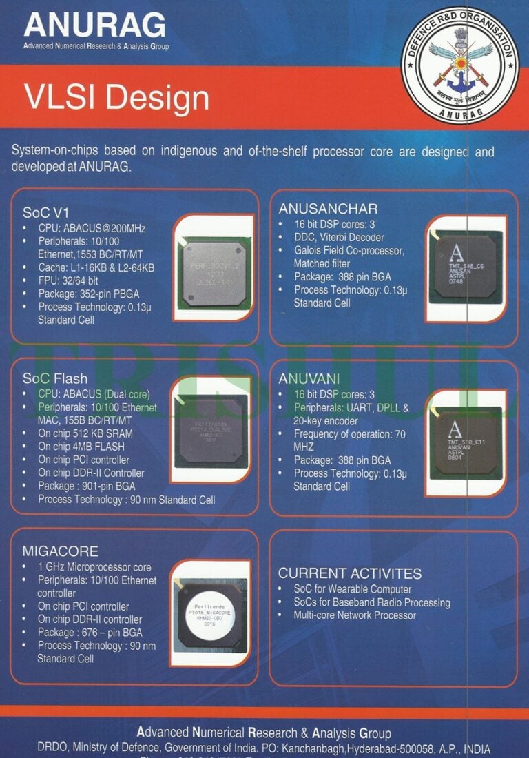
Edv5hVJUcAAat5u-768x1100.jpg


ANURAG designed & manufactured SoC chips for communication systems based on their own & imported processor cores. Photo from 2013. Photo Credit: Trishul blog


By 2013, GAETEC was able to operationalize Standard Cell technology of 130 & 90 nm node, assuming the poster above showcases GAETEC’s best capabilities at that time. The 90 nm Standard Cell tech could be used to fabricate Single/Dual Core 16/32/64 bit processors. Open source RISC architecture was preferred over Intel’s proprietary x86 architecture. The most powerful core available then was the 1 GHz MIGACORE.
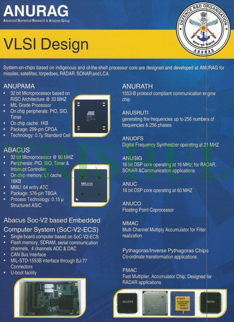

Edv5heVUMAE61se-768x1056.jpg


Evidently the Ball Grid Array (BGA) was the preferred chip packaging technology. Various pin configuration (from 299 pins to 901 pins) were used depending on the size of the processor.

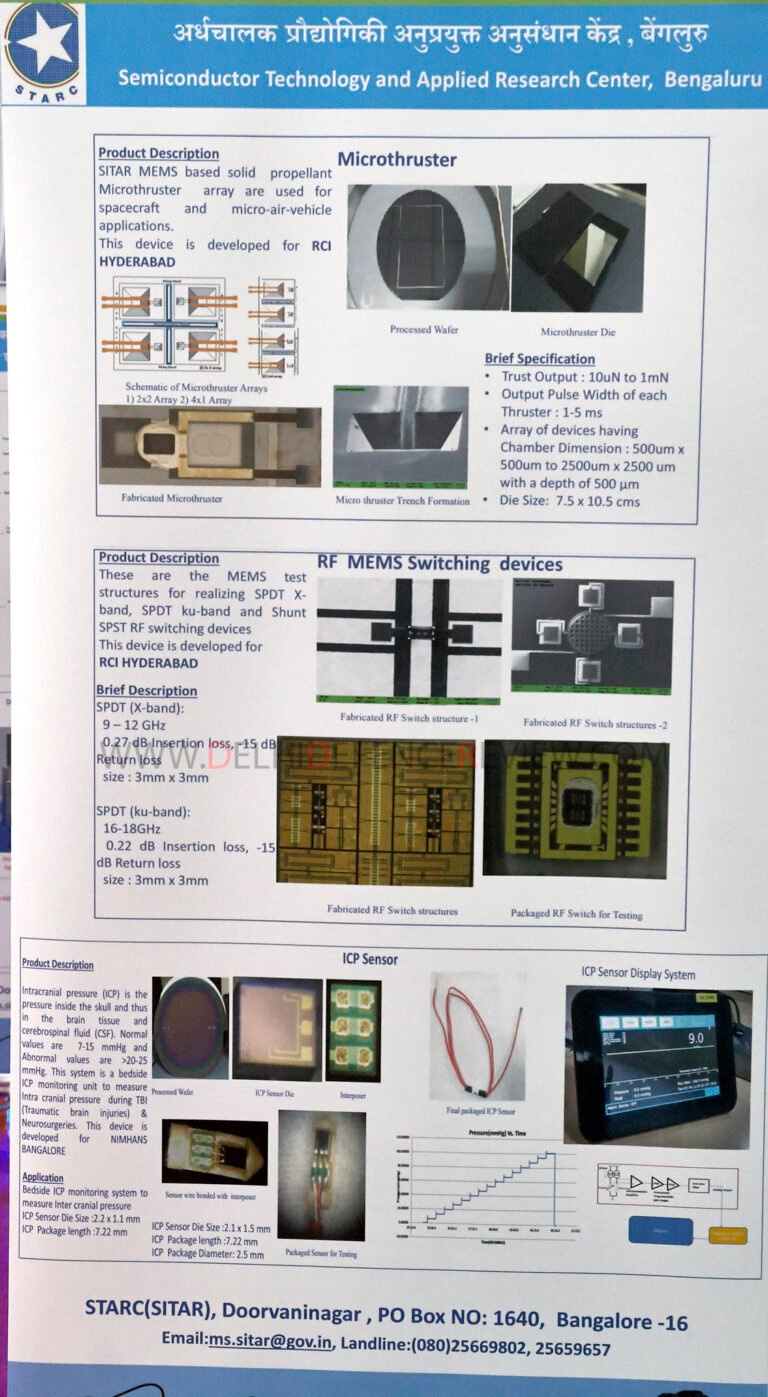
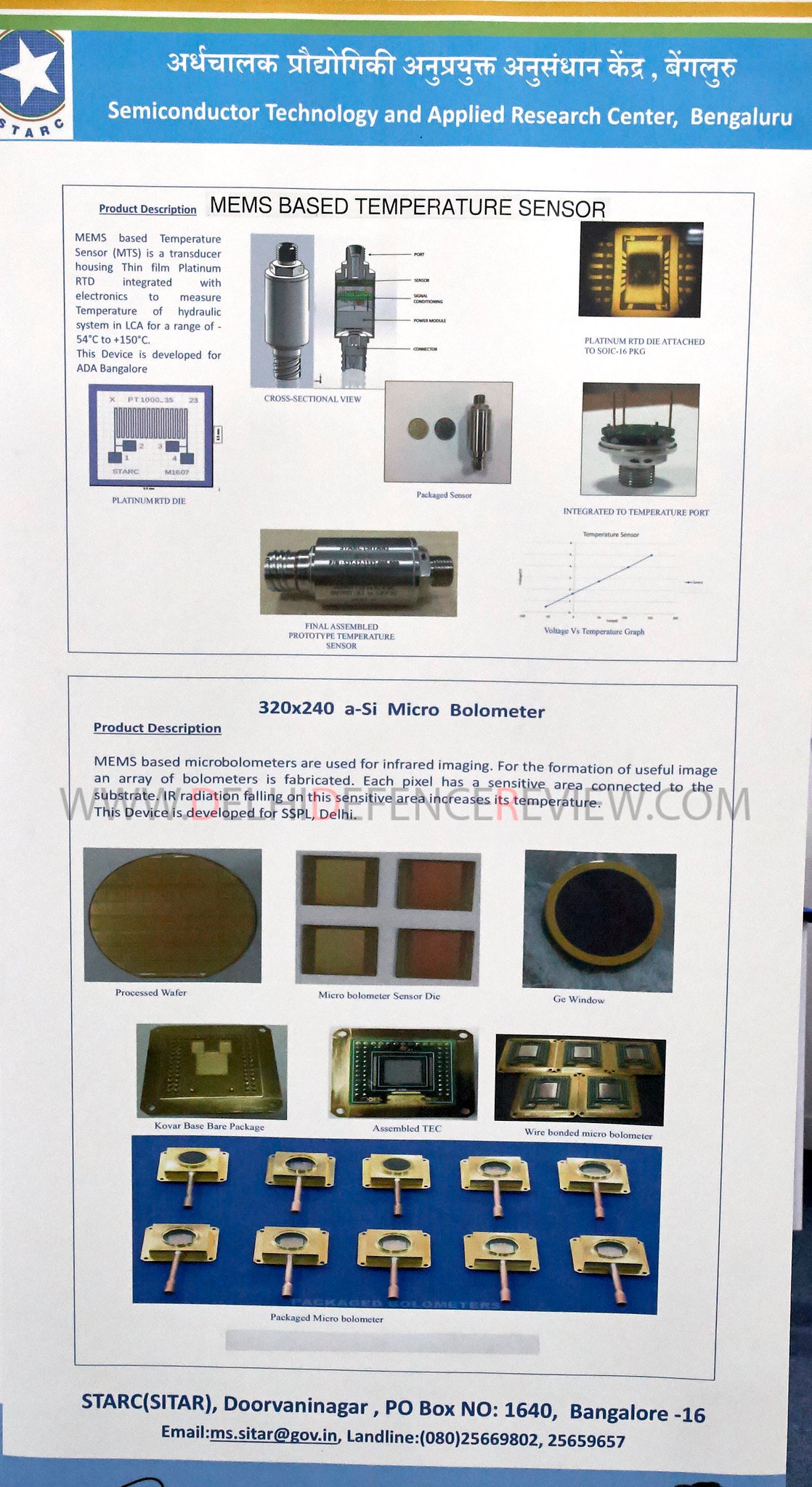
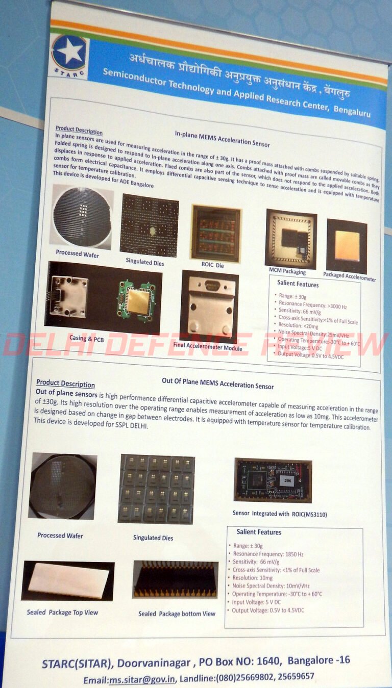
STARC showcased various sensors that are operational now in satellites, RF & IR guided missile seekers.
Evidently the Ball Grid Array (BGA) was the preferred chip packaging technology. Various pin configuration (from 299 pins to 901 pins) were used depending on the size of the processor.

STARC showcased various sensors that are operational now in satellites, RF & IR guided missile seekers.

Edv5hvOVoAAe_ll-768x1397.jpg


STARC made MEMS based micro-thruster for space applications & RF switching systems. The RF switching systems are for X-band & Ku-band radar seekers. Photo Credit: DDR

Edv5h4_UMAACxvc.jpg


STARC made pressure transducer for underwater applications. Photo Credit: DDR

Edv5iL7U8AEGyEx-768x1349.jpg


The current production capacity of the GAETEC & STARC facilities are unknown. In the media, over the last decade, there has been an information gap about the developments in the defence semi-conductor realm. At least some of that is driven by a deliberate policy of secrecy.

While, in the early 2010s, there was some talk of DRDO developing more advanced fabrication technology; there were hardly any specifics mentioned & the news died down.

AMBAR-65-nm-768x605.jpg


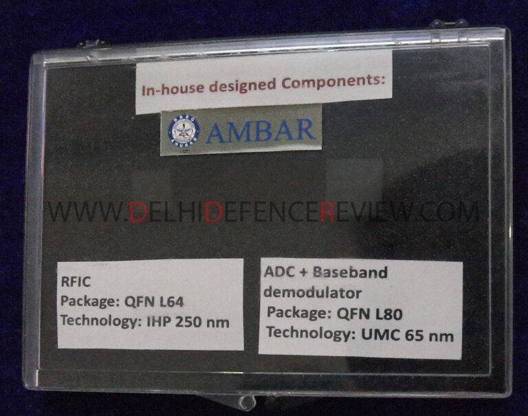
In DefExpo-2018 DRDO displayed an S-band Radio Frequency Integrated Circuit (RFIC) fabricated at IHP’s 250 nm fab in Germany. They also showcased a ADC+Baseband radio chip fabricated at UMC’s 65 nm fab in Taiwan. These chips are meant for a Digital Multi-media Broadcast (DMB) SATCOM terminal. Photo Credit: DDR

To be continued.
 

asaffronladoftherisingsun

Dharma Dispatcher
New Member
Joined
Nov 10, 2020
Messages
12,207
Likes
73,694
Country flag
[]Continued... from https://defenceforumindia.com/threads/bharats-semiconductor-research-efforts.83228/

In this context, the DefExpo-2018 was an absolute goldmine for defence enthusiasts. DRDO displayed a plethora of their work in the semi-conductors, micro-processors, micro-controllers, micro-sensors etc.

L-band-chip-SAC-ISRO-768x1143.jpg


DRDO’s L-band Synthetic Aperture Radar (SAR) chips fabricated at GAETEC, India. These chips were used on the L-band SAR of the DFSAR on the Chandrayaan-2’s orbiter. Photo Credit: DDR.

SICs-MEMS-768x475.jpg


Various other DRDO designed & fabricated chips showcased at the DefExpo-2018. Photo Credit: DDR.

IIT-Mandi had in 2012 developed Photoresists with 20 nm node. This was demonstrated for resolution of 20 nm under EUV (extreme ultraviolet lithography) at Lawrence Berkeley National Laboratory, USA.[3]

IIT-Mandi and various other institutions received funding from MeitY for further developing of sub-10 nm photoresists. IISc has been modifying the well known Glancing Angle Deposition (GLAD) method for depositing sub-10 nm thickness nanomaterials since 2013.[4]

In 2017, IISc’s Centre for Nano Science and Engineering (CeNSE) received Rs 3,000 crore (>US $400 million) funding from DRDO’s SSPL to create a lab-scale foundry for fabricating GaN transistors on Si wafers.[5] In 2018, IISc developed a method for improving the reliability & operating limits of sub 14 nm Ultra-Dense FinFET System-on-Chips (SoCs).[6] While it is not known what tech node SSPL’s lab scale foundry is based on, anecdotal evidence suggests that it is a sub 14 nm FinFET technology.

By 2019, DRDO’s investment into CeNSE started paying off. The IISc had developed & fabricated India’s first-ever 600V class e-mode gallium nitride (GaN) High Energy Mobility Transistors (HEMTs) with performance comparable to some of the best globally. CenSE also developed GaN Schottky diodes.[7]

BEL-X-band-AAAU-plank-GaAs-768x274.jpg


GaAs semi-conductor based plank for the Active Antenna Array Unit (AAAU) of the Uttam AESA radar. There is a GaN based AAAU under-development. Photo Credit: DDR.

The CeNSE’s fabrication technology has been transferred to SSPL who intends to used the HEMTs in high powered AESA radars, EW systems & military communications systems.

In early 2021, the prototyping phase of the projects has begun. We are likely to see GaN based HEMTs operationalized in the next couple of years.

Solid State Physics Lab has issued a tender for production of 10 GaN HEMTs on 4 inch Si substrates. DRDO has been working on GaN HEMTs for next gen radars as they are more powerful & efficient compared to the currently used GaAs. It seems prototyping phase of GaN HEMT has begun. pic.twitter.com/1WIckXSDmQ
— Strategic Frontier (@strategic_front) May 16, 2021
In October 2021, the Ministry of Defence (MoD) had announced that Astra Microwave Pvt. Ltd. & BEL were given an order to supply 1 unit each of the Uttam Mark-2 radar by April 2022. The Uttam radar is an airborne X-band AESA radar designed by DRDO’s LDRE for the HAL Tejas Mk-1A fighter.

The Uttam Mark-2 is an upgraded version of the base Uttam radar that features a larger aperture for more Transceiver Receive Modules (TRMs) & is meant to be used in the upcoming HAL Tejas Mk-2 fighter. The Uttam Mk-2 is also likely to feature GaN semi-conductors instead of the GaAs used on the Uttam.

In December 2021, the MoD has released a Process Design Kit (PDK) for companies, start ups & entrepreneurs interested in designing GaN MMICs & getting them fabricated at GAETEC. [8] This obviously demonstrates that GAETEC had fully established GaN semi-conductor manufacturing capability by then.

DRDO’s efforts in the micro-controller & micro-processor space created the critical mass of experience needed to get other major players interested. The other major player here is the Indian Space Research Organisation (ISRO).

Space
ISRO had for long desired the use of their own chips in space missions. But they had to rely on imported ones as the barrier to entry, both technologically & monetarily were very high. ISRO had used the American made Motorola 6800/6809 and Intel i960 based processors for navigation, guidance & control tasks on their Onboard Computers (OBCs) for space launch vehicles for a long time.

Like DRDO, ISRO too had set up a semi-conductor making unit called Semi-Conductor Laboratory (SCL) in the 1980s. In the early years, SCL did packaging work on the imported American chips. As their experience & competence in VLSI design grew, SCL started designing chips to have them manufactured abroad.


Edv5io7U4AAYP63-768x322.jpg


Wafer fabrication site at SCL, Chandigarh. Photo Credit: ISRO

ISRO set out to design a micro-processor on their own a few years back. It was named “Vikram 1601” after ISRO’s founder Dr. Vikram Sarabhai.

Edv5ifoU8AAo_yd.jpg


Vikram 1601 processor. Photo Credit: ISRO


The processor was designed & fabricated by the Semi-Conductor Laboratory (SCL) at Chandigarh using 180 nm Complementary Metal Oxide Semiconductor (CMOS) technology. The processor has a 16 bit, RISC-V architecture with a base clock speed of 80 Mhz. There is a 32 bit variant being made too.

Edv5iwrU0AAk1FT-768x743.jpg


Inside SCL’s wafer fabrication site. Photo Credit: ISRO


ISRO has already put the Vikram 1601 processor to use in their next generation OBCs. Starting with the PSLV-C47 mission that put the CARTOSAT-3 in orbit, all missions from then on used the Vikram 1601 processor.[9]

SCL-1200x357.png


Some of ISRO’s more recent chips used on various space missions. Photo Credit: ISRO

ISRO, like DRDO, went with the open source RISC-V architecture for their semi-conductor designs. It would be interesting to see if either of these two show any interest in developing their own proprietary architectures in the future.

SCL2-1200x392.jpg


ISRO, like DRDO, went with the open source RISC-V architecture for their semi-conductor designs. It would be interesting to see if either of these two show any interest in developing their own proprietary architectures in the future.

However, unlike the DRDO, ISRO has managed to find a way to scale up the semi-conductor fabrication at SCL. ISRO has found an unlikely customer in the Indian Railways.

The Railways is undergoing a great change in the last few years. They are electrifying the entirety of their network & will eventually de-commission most if not all of their old diesel engines. Besides the reduction in pollution railway electrification will significantly reduce the India’s oil import bill. As of 1st April 2021, they have already electrified ~63 % of their total network & are aiming for 100% electrification by 2024.

The electrification has obviously caused a massive demand for many electronic components including semi-conductors. ISRO’s SCL has managed to capitalize on some of that demand. SCL has supplied chips for control electronics of electric locomotives, Track Management Systems (TMS) & indigenous Automatic Train Supervision (i-ATS) for metro rail.

However, unlike the DRDO, ISRO has managed to find a way to scale up the semi-conductor fabrication at SCL. ISRO has found an unlikely customer in the Indian Railways.

The Railways is undergoing a great change in the last few years. They are electrifying the entirety of their network & will eventually de-commission most if not all of their old diesel engines. Besides the reduction in pollution railway electrification will significantly reduce the India’s oil import bill. As of 1st April 2021, they have already electrified ~63 % of their total network & are aiming for 100% electrification by 2024.


The electrification has obviously caused a massive demand for many electronic components including semi-conductors. ISRO’s SCL has managed to capitalize on some of that demand. SCL has supplied chips for control electronics of electric locomotives, Track Management Systems (TMS) & indigenous Automatic Train Supervision (i-ATS) for metro rail.

Screenshot-280-768x1196.png


SCL designed & fabricated chips for new Indian Electric Locomotives. Photo Credit: ISRO

SCL might also supply the chips needed for the RDSO designed Train Collision Avoidance System (TCAS) if & when it gets deployed nationwide. The TCAS is currently being field tested.

In 2016, SCL in collaboration with IIT-Bombay started augmenting the currently used 180 nm CMOS fab with Bi-CMOS technology. Bi-CMOS (short for Bipolar-CMOS) technology enables fabrication of mixed signal ICs. It combines 2 transistor technologies in one chip – the high-speed and high power Bipolar Junction Transistor (BJT), and low speed and low power Complementary Metal Oxide Semiconductor (CMOS). The result is a versatile technology platform in terms of integrated digital-analog (i.e. mixed) signal ICs, with optimal performance based on choice of high speed (BJT) and low power (CMOS), which enables IoT applications.[10]

Also, ISRO’s Satellite Application Centre (SAC) reportedly did some R&D work on 70 nm fab.[3] In 2020, ISRO announced that it is looking to build an additional fab at their SCL facility. The new fab will have 65 nm node. It is not known if the fab will used CMOS tech or any other technology. It is also not known when the new fab will come up.[11]

To be continued.
 
Last edited:

asaffronladoftherisingsun

Dharma Dispatcher
New Member
Joined
Nov 10, 2020
Messages
12,207
Likes
73,694
Country flag
[]Continued... from https://defenceforumindia.com/threads/bharats-semiconductor-research-efforts.83228/


Academia
In recent years, various branches of the GoI has sponsored the development of micro-processors by academia for various applications. Many of India’s top engineering institutes have already developed silicon proven chips. The chips we’ve seen so far.

IIT Bombay
IIT-Bombay developed the AJIT microprocessor with funding from Ministry of Electronics and Information Technology (MeitY) & Powai Labs. Powai Labs is a company incubated within the IIT-Bombay campus. They plan to commercialize the chips developed by IIT-Bombay.

The AJIT processor is meant to be used on WiFi routers, smart electric meters and Electronic Voting Machines (EVMs) etc.[12]

The processor has a clock speed of 70-120 MHz, using the SPARC ISA & is built on 180 nm CMOS technology at SCL. Clock speeds of 400-500 MHz is achievable in the next upgrade.

Edv5jAmUcAAs0kb-768x721.png


AJIT micro-processor was designed by IIT-Bombay and fabricated at ISRO’s SCL. Photo Credit: IIT-Bombay

The processor can also be used in set-top boxes, in control panels of automation systems, in traffic light controllers and in robotic systems. Plans are underway to use AJIT in receivers being developed for NAVIC/IRNSS. It is expected to cost just ₹100/processor when it is produced on a larger scale.

Edv5jSAUcAcKPKa.png


The AJIT micro-processor has 208-pin Ceramic Quad Flat Pack(CQFP) type packaging. It has a size of (12 x 12) square mm. Photo Credit: IIT-Bombay


IIT-Bombay has also developed a receiver chip for navigation purposes meant to be used in mobile phones, tablets etc. It is named “Dhruva”. Dhruva will receive signals from India’s NAVIC group of navigation satellites as well as the US Global Positioning System (GPS) satellites to determine locations accurately under all weather conditions.

Ef_qkZeXsAEw4A4-768x512.jpg


The Dhruva Quad Flat no-Leads(QFN) packaged chip on a fingernail. Photo Credit: IIT-Bombay

The Dhruva project was also funded by MeitY, with the Society for Applied Microwave Electronics Engineering and Research (SAMEER) acting as the nodal agency. The research team also interfaced with the Space Applications Centre (SAC) of the ISRO.[13]

Ef_qkUTWkAARhsX-1-768x764.jpg


Photo of the die of the Dhruva chip. The chip was fabricated on 65nm CMOS tech with die-size (1.8×1.8) square mm. Photo Credit: IIT-Bombay

It is not known where the test chips were fabricated. The chip is developed as a production-level IC with ESD protection, on-chip testing, and reference circuits operating from -40 to 100 °C. The IC consumes a maximum of 60 mW from a 1.2 V power supply, which is comparable with the existing commercial navigation chips.

Ef_qkY-X0AA53zS-768x574.jpg


The test chip mounted on the PCB. Photo Credit: IIT-Bombay

After fabrication the chip was mounted on to a PCB and tested. In the tests the chip managed to tune into signals at multiple frequencies like the 1.175 GHz (NAVIC – L5 band), 1.227 GHz (GPS – L2 band), 1.575 GHz (GPS – L1 band) & 2.492 GHz (NAVIC – S band).


Ef_qkUoWAAASE4a-768x538.png


Signals received by the chip from American GPS satellites during test. Photo Credit: IIT-Bombay

Once the Indian government mandates the use of NAVIC for mobile & commercial applications, Dhruva can be integrated into commercial implementations.

To be continued.
 

asaffronladoftherisingsun

Dharma Dispatcher
New Member
Joined
Nov 10, 2020
Messages
12,207
Likes
73,694
Country flag
[]Continued... from https://defenceforumindia.com/threads/bharats-semiconductor-research-efforts.83228/


IISc Bangalore

file791lfi8fjirxp2hyq-768x512.jpg


IISc designed & fabricated TWR radar on chip. Photo Credit: ARSL, IISc

In 2020, researchers at the Indian Institute of Science (IISc) have developed a “through-the-wall” radar (TWR) built on a chip. Developed using Complementary Metal Oxide Semiconductor (CMOS) technology, this radar has a single transmitter, three receivers, and an advanced frequency synthesizer capable of generating complex radar signals, all packed together into a tiny chip smaller than a grain of rice.

insignifican-768x576.jpg


A photomicrograph of the TWR radar-on-chip compared to a grain of rice. Photo Credit: ARSL, IISc

“TWR imaging has always been one of the most challenging radar design problems,” says Banerjee. For one, the signal can get significantly damped while passing through walls. To overcome this, radio waves consisting of a large number of frequencies need to be used, which can complicate the design. These radars also use a more complex signal, known as a chirp, which requires customized electronics such as a microwave transmitter, a receiver and a frequency synthesizer.

1580222071849.png


An FMCW chirp generated by the transmitter. Photo Credit: ARSL, IISc


With their design, the IISc team has now managed to squeeze all of these electronic components into a single, tiny chip. They used new architectural and circuit design techniques to overcome challenges specific to radars – such as the design of a wide fractional bandwidth transceiver. “The same design techniques that have enabled smaller and cheaper smartphones can now be used to miniaturize the complex electronics of a radar system into a small chip,” says Gaurab Banerjee, Associate Professor at the Department of Electrical Communication Engineering, IISc.[14]

Image-2-768x1024.jpeg


Radar-on-chip : The packaged chip is smaller than a one-rupee coin and chip itself is slightly smaller than a grain of rice. Photo Credit: ARSL, IISc

This research was funded by the IMPRINT program of the GoI, with additional financial contributions from the Ministry of Human Resource Development (MHRD) and the DRDO. Bharat Electronics Limited (BEL) has been an active industrial partner in this IMPRINT project since its inception.

BEL currently supplies the military with their Through Wall Radar (TWR). The TWR has found acceptance among various CI/CT units of the military that frequently engage in CQB.

see-rad-1-768x658.jpg


BEL TWR showcased at the DefExpo 2018 event. Photo Credit: DDR

BEL TWR was first showcased to the public at the DefExpo 2018. The radar operates in the C-band with a bandwidth of >500 MHz. It has a refresh rate of 12 frames per second. The TWR carries a 480×360 screen to display the radar generated image. It can operate through walls made of cement plaster, 9 inch bricks, concrete, RCC slabs, stones, mud, wood etc.

lrde-product-images-16.jpg


LDRE developed Through Wall Imaging Radar (TWIR) was licensed to BEL for production & sale. Photo Credit: LDRE, DRDO.

The BEL TWR seems to be a lightweight version of the LDRE developed TWIR. LDRE licensed the production & sales of the radar to BEL. BEL in turn seems to have modified the design to make it more portable.

The BEL TWR uses an ALTERA Stratix II FPGA family based on Intel’s processors fabricated using 90 nm tech node.[15] ALTERA is an American company owned by Intel.


Screenshot-592-768x575.png

Multi-channel Signal processing board used on the BEL TWR.


In this context the development of the IISc’s miniaturized radar-on-chip is significant. For BEL the new chip could be a way of further reducing the size of the TWR & also reducing its price. For IISc the involvement of BEL should mean quicker commercialization of their tech.

To be continued.
 

asaffronladoftherisingsun

Dharma Dispatcher
New Member
Joined
Nov 10, 2020
Messages
12,207
Likes
73,694
Country flag
[]Continued... from https://defenceforumindia.com/threads/bharats-semiconductor-research-efforts.83228/ https://defenceforumindia.com/threads/bharats-semiconductor-research-efforts.83228/post-2131145 https://defenceforumindia.com/threads/bharats-semiconductor-research-efforts.83228/post-2131147

IIT Hyderabad
In March of 2019 researchers from the Advanced Embedded Systems and IC Design Laboratory, Department of Electrical Engineering, IIT Hyderabad & and University of Hyderabad (UoH) fabricated a IC chip made of magnetic Graphene. [16]

Later in October of 2019, IIT Hyderabad announced that they have developed ultra low power magnetic chips to be used on portable AI applications.

The chips were developed using Magnetic Quantum-dot Cellular Automata (MQCA) based nano-magnetic logic architectural design methodology.[17]

In 2021, IIT Hyderabad, NXP India and MeitY joined hands for the launch of the first “Semiconductor Startup Incubation and Acceleration Program”. Under this program IIT Hyderabad will provide semi-conductor design start ups with free access to highly expensive EDA tools and prototyping, apart from the basic infrastructure.[18]

IIT Delhi
In 2018 IIT-Delhi started a partnership with Weebit Nano, an Israeli company developing ReRAM. ReRAM or Resistive RAM are one of the candidates for next generation high speed Non-Volatile Memory (NVM).

Re-RAM use neuromorphic computing architecture is a type of Non Von Neumann Architecture. Neuromorphic computing architecture, unlike traditional Von Neumann Architecture is not constrained by the limits of Moore’s Law.

IIT-Delhi has set up a Non-Volatile Memory Research Group (NVMRG) to work jointly with Weebit Nano on the Neuromorphic ReRAM project. [19]

IIT Madras
IIT Madras has the most extensive semi-conductor development plan of all research institutions in the country. It started as an academic initiative in 2014 to create an ecosystem of production grade processors, SoCs & peripheral IPs using open source ISA by the Reconfigurable Intelligent Systems Engineering (RISE) group at IIT-Madras.

The RISE group got financial backing from the MeITY & technology support from HCL Technologies & Intel Corp. The RISE group aims to build 6 variants of processors based on the RISC-V ISA. The family of processors was named “SHAKTI”.

The SHAKTI processors family can be broadly categorized into 3 broad groups, each with their own sub-groups. The categories are:

Base Processors
Base processors are the building blocks for the SHAKTI family. They are all single core processors. The Multi-Core processors will be created by combining the base processors. Thus the entire project hinges on the success of these processors. There are 3 types of base processors being developed.

1. E class (70 MHz – 500 MHz): 32/64 bit micro-controllers for low power & low speed computing applications like smart-cards, IoT devices, motor controls & robotics. Development of the processors is complete. Multiple processors have been fabricated for testing.

Currently System on Chips (SoCs) are being tested built around the E-class core. E-arty35T is an SoC built around the 32-bit E-class microcontroller with 128KB RAM. The development of the SoCs are being conducted on commercially available FPGA development boards from Xilinx.

In mid-2020, the “MOUSHIK” SoC became the 1st E-class SoC of the SHAKTI family to be fabricated. It is also the only E-class SoC fabricated till date. The MOUSHIK was fabricated at ISRO’s SCL on the 180 nm CMOS node. It has a size of (5.315×5.155) mm2, speed of 100Mhz & is packaged using 256 pin Ceramic Quad Flat Pack (CQFP) technology.[21]

chip1_5f6dae6ed5c82-1-165x220.jpg


MOUSHIK SoC. Photo Credit: RISE Group, IIT-Madras

The SoC is targeting a wide variety of use cases like Credit cards, ID Cards, Debit cards, Travel Cards for Metros and Driving Licenses, EVMs, Office Management Systems including Attendance, CCTV cameras, Safe locks, Consumer Electronics including but not restricted to Washing Machines and Water pump monitoring systems etc.

‘Ardonyx_1.0_an_indigenously-developed_motherboard_with_the_MOUSHIK_Microprocessor_-1-2-1200x900.jpg


RISE/HCL Ardonyx MS Version 1.0 motherboard with SHAKTI processor. Photo Credit: RISE Group, IIT-Madras


The RISE Group along with HCL Technologies designed a motherboard named “Ardonyx MS Version 1.0” for the MOUSHIK. There are more advanced motherboards being designed for other SHAKTI processors.

Video of Post-Silicon Boot-up were done at IIT Madras


2. C class (500 MHz – 1.5 GHz): 64-bit micro-controllers for mid-range embedded applications like data storage, hardware networking, gateways etc. C-arty100T is a SoC built around the C-class. The C-arty100T SoC is a single-chip 64-bit C-class microcontroller with 128MB DDR3 RAM.

These processors are nearing the end of their development. Two variants of the C-class processors have been fabricated for testing. The two variants are called : RIMO & RISECREEK.

RISECREEK : This was the 1st chip from the SHAKTI family to be fabricated. Fabrication work was done at the Intel’s Oregon, USA facility using 22 nm FinFET technology in late 2017.

Edv5l3JUMAAGSeg.jpg


Bottom side(LEFT) & Top side(RIGHT) of the RISECREEK processor. Photo Credit: RISE Group, IIT Madras

RISECREEK is a (4×4) mm2 sized processor featuring a 208-pin Ball Grid Array (BGA) type packaging. The initial test chips were intended to validate the VLSI design, thus the clock speed was restricted to 350 MHz.

Edv5l-DVAAEkihR-768x576.jpg


Multiple RISECREEK processors were fabricated at the Intel’s Oregon facility. Photo Credit: RISE Group, IIT Madras.

The RISECREEK processor drew a lot of attention form some nuclear & space research institutions. These institutions include :

  • Indira Gandhi Centre for Atomic Research (IGCAR)
  • Bhabha Atomic Research Centre (BARC)
  • ISRO Inertial Systems Unit (IISU)
These institutions saw the RISECREEK’s capability, its RISC-V ISA & its customizability in very positive light. And the fact that the IP was entirely Indian wasn’t lost either.

ICGAR & BARC under the Department of Atomic Energy (DAE) drew up a road map to implement the SHAKTI processors in the Computer Based Instrumentation & Control Systems (CBS) of Indian nuclear reactors.

Screenshot-594-768x427.png


Roadmap for implementation of SHAKTI processors in the CBS of Indian nuclear reactors. Photo Credit: ICGAR & IIT-M presentation.

The reactors in question are the Indian designed & built Pressurized Heavy Water Reactors (IPHWR-220) & the Prototype Fast Breeder Reactor (PFBR) based at the Madras Atomic Power Station (MAPS).

Screenshot-596-768x473.png


Prototype development roadmap. Photo Credit: ICGAR & IIT-M presentation.

If this projects succeeds then there are plans to used the SHAKTI processors on other Indian reactors namely the IPHWR family (220, 540, 700) & upcoming reactors like the IPWR-900, FBR-600, AHWR-300 etc.

All Indian nuclear reactors currently use domestically designed CPU cards based on Motorola MC68020 processors with a speed of 25 MHz.

image.png


If this projects succeeds then there are plans to used the SHAKTI processors on other Indian reactors namely the IPHWR family (220, 540, 700) & upcoming reactors like the IPWR-900, FBR-600, AHWR-300 etc.

All Indian nuclear reactors currently use domestically designed CPU cards based on Motorola MC68020 processors with a speed of 25 MHz.


Following the tech development roadmap piggy back boards had been developed by 2018. Piggy back boards were used to test the ability of the RISECREEK processors to handle the computing operations as needed. The Motorola powered CPU boards were used as a fail safe, in-case, the RISECREEK fails.

Picture2.png


SHAKTI back board built using Xilinx Artix 7 FPGA. Photo Credit: ICGAR & IIT-M presentation.

These piggy back boards were initially tested in isolation & then with the whole systems. Testing continued for 2 years, the boards proved to be reliable & were seen as potential replacements to the MC68020 VME bus based CPU cards.

Edv5mnOU8AAoxc1-768x299.png


Piggy back board with sockets for MC68020 & RISECREEK. Photo Credit: ICGAR & IIT-M presentation.

By mid-2019, multi-channel Analogue & Digital Input Cards (AIC & DIC) were fabricated & tested. Analogue & Digital Output Cards (AOC & DOC) were also being tested. These cards were also powered by SHAKTI processors.

Screenshot-597.png


Digital & Analogue Input/Output Cards powered by SHAKTI processors. Photo Credit: ICGAR & IIT-M presentation.

To be continued.
 

asaffronladoftherisingsun

Dharma Dispatcher
New Member
Joined
Nov 10, 2020
Messages
12,207
Likes
73,694
Country flag
[]Continued.. from https://defenceforumindia.com/threads/bharats-semiconductor-research-efforts.83228/post-2131161

Since the currently used Motorola MC68020 & the SHAKTI processors have different architectures (CISC vs. RISC V), Human-Machine Interface (HMI) software had to be developed for making them compatible. Diversified systems were built for testing the software & the compatibility of the American & Indian processors.
Screenshot-595-768x356.png


Diversified System consisting of both Motorola & SHAKTI processors. The systems was built to test the compatibility of the processors using a HMI software. Photo Credit: ICGAR & IIT-M presentation.

By late 2019, Computer Based Instrumentation & Control Systems (CBS) completely based on SHAKTI SoCs began development. This is the last stage of the ICGAR’s roadmap for adopting SHAKTI processors.

Screenshot-593-768x521.png


SHAKTI SoC based CBS for new nuclear reactors. This photo shows the systems that controls the Reactor Start up Authorization Logic. Photo Credit: ICGAR & IIT-M presentation.

In late 2020 some media houses reported that the RISECREEK is already in use in India’s strategic sector.[21]

RIMO : RIMO is the 1st member of the SHAKTI family of processors to be fabricated in India. It was fabricated at SCL using 180nm CMOS technology in late 2018. The RIMO is a (12 x12) mm2 64-bit microcontroller featuring a 208-pin Ceramic Quad Flat Pack(CQFP) type packaging. The test chip had a maximum clock speed of 70 MHz.
Edv5lmnUwAEOXSU.jpg


RIMO processor. Photo Credit: RISE Group, IIT Madras.

Multiple chips have been fabricated at the SCL for testing, hardware & software developments.

Edv5lstU4AUU-FA-1.png


A later production model of the RIMO processor. Notice the number “19” hand written on the chip. Photo Credit: RISE Group, IIT Madras.

The test boards were designed by HCL Technologies and IIT Madras & were fabricated by another Indian company called Ohm CAD systems.

Edv5lBEUwAAOr6X-165x220.jpg


RISE/HCL designed test motherboard with RIMO processor mounted. Photo Credit: RISE Group, IIT-Madras

In DefExpo 2020, IIT Madras had announced that significant progress had been made on the indigenous processor. IIT-M is now building the next generation of Artillery Combat Command and Control Network for the Indian Army. The fire control network has been proposed to be based on a Shakti processor in a lightweight tablet configuration. It will be a precursor to secure net-centricity in the Armed Forces incorporating all-new weapon systems.[22]

3. I class (1.5 GHz – 2.5 GHz): These are 64-bit single core superscalar Out-of-Order (OoO) processors which targets the Smartphones, tablets laptops, high-end storage & networking devices etc. Design work of the 1st I class processors had been completed by 2020. The RISE Group is targeting 1 GHz clock speed in the 1st chip to be fabricated. The fabrication will be on Intel’s 22 nm FinFET technology. Once the test chip is fabricated & the design is verified, SoCs based on the I class will be developed.[23] As of 2021 there has been no further updates on the I class.

Multi-Core Processors
The SHAKTI family of processors will extend out to Multi-core processors in the future. These processors will use a combination of the base cores of the SHAKTI. The development of these processors will begin after the base cores are fully developed.

  1. M class (Upto 2.5 GHz): These are 64-bit processors that can support up to 8 cores. The cores will be a combination of C & I class cores. The M-class processors are intended to be used on desktop workstations, mid/high end laptops & modems.
  2. S class (>3 GHz): The S-Class is a 64-bit superscalar, multi-threaded processor aimed at workstations, enterprise server application, data centers etc. Its supports 2-16 cores where the base core is an enhanced version of the I-class.
  3. H class (?? GHz): The H-class is a 64-bit processor aimed at highly parallel enterprise, supercomputing and analytics applications. The cores can be a combination of C or I class, single-thread performance driving the core choice. The H-class can support up to 128 cores with multiple accelerators per core. The clock speed of H-class processors have not been revealed.
Experimental Processors
The SHAKTI family will also have some experimental/research processors. These experimental processors would focus on being highly secure and fault tolerant. They are based on the SHAKTI base cores.

1. F class: The F-class is a fault-tolerant version of the base C class processor. It features include redundant compute blocks (like DMR & TMR), temporal redundancy modules to detect permanent faults, lock-step core configurations, fault localization circuits, ECC for critical memory blocks and redundant bus fabrics.

The F class processors are designed keeping in mind the needs of the automotive, healthcare, industrial control, avionics & space industries in mind.

Screenshot-598-768x373.png


Graph showing use cases of processors based on safety vs. time criticality. The application area marked by the grey circle is being targeted by the SHAKTI F class processors.

The F class processors drew interest from the French multi-national company Thales’ Avionics division. Thales funded the development of a Mixed Critical SoC based on the F class processor to be used on RV avionics.[24][25] The quantum of funding remains unknown.

shakti_week_SafeRV-split5_page-0001-1200x675.jpg


Block diagram of the SHAKTI-Thales Safe RV Mixed Critical SoC based on the F class. [23]

In a paper published by IIT Madras at the 2015 IEEE 24th Asian Test Symposium, it was shown through simulations that a F class processor fabricated on a 55 nm technology node would run at 330 MHz.[26]

Screenshot-599-768x770.png


The simulated layout of the SHAKTI F-class core using 55 nm technology.

The researchers add that this is sufficient for the applications that these F class cores are meant to be utilized for. Besides the operating speed can be increased easily if 22 nm or smaller nodes is used. It is not known if any F class processors were fabricated yet.

2. T class: The T-class is aimed to provide additional hardware support for securing information from memory-based attacks. Its design focuses on a unified hardware framework for mitigating spatial and temporal memory attacks.

These processors are also based on the SHAKTI C-class processors. But the enhancements/modifications devised to convert the C-class to T-class can be used on other base processors as well.

ArjunMenon_MAST2019-split_page-0001-768x731.jpg


Vulnerabilities of a processor that can be attacked & the ongoing research to prevent/mitigate such attacks. Photo Credit: RISE Group, IIT-Madras presentation.

The T-class processors are meant to be used for handling highly sensitive information. Thus they are built to prevent/mitigate information losses & withstand all forms of cyberattacks.

ArjunMenon_MAST2019-split_page-0003-768x432.jpg


Comparison of the SHAKTI T-class with other similar processors. Photo Credit: RISE Group, IIT-Madras presentation.

To be continued.
 

asaffronladoftherisingsun

Dharma Dispatcher
New Member
Joined
Nov 10, 2020
Messages
12,207
Likes
73,694
Country flag
[]Continued... from https://defenceforumindia.com/threads/bharats-semiconductor-research-efforts.83228/post-2131169


For attaining requisite levels of information safety vulnerabilities across the spectrum need to be addressed. The vulnerabilities can be in the software, micro-architecture & the hardware. Each of these categories of vulnerabilities are separately addressed during research.

For prototyping & testing it seems they have consolidated the software & micro-architecture categories. The resulting prototype chip is called the SHAKTI-MS processor. MS stands for Memory Safety.[27]

For addressing the vulnerabilities of the processor to power based attacks, that can steal information passing through the chip using hardware, the base C-class chip had to be redesigned. The test chip for withstanding hardware based vulnerabilities was named: Power-Attack Resistant Microprocessor (PARAM).
Arjun_MAST2019-split_page-0007-768x432.jpg


Data leakage analysis of SHAKTI C-class base processors. Photo Credit: RISE Group, IIT-Madras.

The vulnerability of the base C-class to power based attacks were assessed via simulations and physical testing. The photo above shows the finding of those tests

The regions marked in red show a near 100% leakage of data passing through them. The regions marked in yellow indicates a data leakage of around 30-60 %.

Arjun_MAST2019-split_page-0009-768x432.jpg


Leakage mitigation on the SHAKTI C-class base processors via the proposed changes. Photo Credit: RISE Group, IIT-Madras.

After the modifications were made the data leakage was significantly reduced. As is shown in the photo above the regions of severe data leakage were significantly reduced though other regions of mild leakage persisted. Further information security can be achieved by a proposed compartmentalization of data.

The comparison of the base SHAKTI C-class processor with the PARAM reveals a stark difference in data security.

Arjun_MAST2019-split_page-0010-768x432.jpg


Security Analysis of the base SHAKTI C-class processor & PARAM. Photo Credit: RISE Group, IIT-Madras.

In 2019, the RISE Group proposed that the next steps in the development of the T-class would be integrating the security features of the SHAKTI-MS & PARAM into a single processor. This would be followed by validating the hardware & software developed & assessing the vulnerability of the processor. Further modifications could be made after the proposed integration.

In 2018, RISE Group formed a start up named “InCore Semiconductors Pvt. Ltd.” to commercialize the processors developed so far. InCore Semiconductor was incubated at IIT Madras. They have agreements with some global semiconductor foundries & have up to 7 nm technology node available to them. It seems InCore aims to be a fabless chip design company like ARM.

In July 2018, speaking at the RISC-V International Workshop held in Chennai InCore’s CTO Neel Gala introduced 3 processors for specialized applications. They were named : AEON, AXON & AEGIS. These are probably the brand names to be used to commercialize some of the chips developed so far.

AEON is the intelligence enabled chip for IoT devices, AXON is the reliability enabled chip for automotive/aerospace uses & AEGIS is the security enabled chip for handling critical data. All 3 chips will use modified E & C class cores.

You can watch Neel Gala’s full presentation here:


In July 2021, it was reported that InCore signed its 1st licensing agreement with the American company Altair. InCore’s chips will be used in embedded applications, robotic controllers, and IoT boards.[28] Judging from the list of applications InCore probably licensed their AEON & AXON processors. The AEGIS will probably find users in the banking, finance, payments, defence etc. markets.

C-DAC

Centre for Development of Advanced Computing (C-DAC) is an autonomous society under the MeitY set up by the GoI in 1988 to develop supercomputers in India. Supercomputers were among the many “dual-use” technologies that were denied to India by the US & other many countries.

Within 2 years of C-DAC’s formation they demonstrated a prototype supercomputer (which would later become the PARAM 8000) at the 1990 Zurich Super-computing show. It was demonstrated that India had the second most powerful, publicly-demonstrated , supercomputer in the world after the United States at that time. The PARAM 8000 was noted to be 28 times more powerful than the Cray X-MP that the GoI originally wanted to buy from the US, for the same $10 million cost quoted for it.

Currently the PARAM family of supercomputers are used by various Indian research organizations working on various technologies for military, nuclear, space, weather mapping, medicine, AI etc. In the last decade various academic institutes manages to purchase various models of the PARAM & establish their own supercomputing centers.

The PARAM supercomputers were also exported to many countries. Ironically some of the customers were the same countries that were part of the technology denial regime. The PARAM has been exported to: Russia, Singapore, Germany, Canada, Tanzania, Armenia, Saudi Arabia, Ghana, Myanmar, Nepal, Kazakhstan, Uzbekistan, and Vietnam.

After the initial success we became complacent. Most of the technology denial regimes were lifted & thus importing supercomputers became common. Investment in domestic capabilities shrunk from the mid-90s. To remedy this MeitY finally came up with a plan. In 2015, MeitY launched the National Supercomputing Mission (NSM) to install 73 indigenous supercomputers throughout the country by 2022. This 7 year program will cost ~US $730 million & will create a high speed link between various new/old academic supercomputing centers called the National Knowledge Network (NKN). The NSM will be done in 3 phases:

PhaseI: Deploying supercomputers with 60% domestic components. (Processors & Motherboards are imported)

PhaseII: Designing processors & Fabricating motherboards. Deploying supercomputers with Indian processors.

PhaseIII: Deploying completely Indian supercomputers.

This is easily one of the most ambitious projects so far for C-DAC. The current status of the project is as follows:

PhaseI: Complete

PhaseII: Will be completed by September 2021. PhaseII will take the country’s computing power to 16 Petaflops (PF).

PhaseIII: Will start this year & will take the India’s computing power to around 45 Petaflops (PF). This will include 3 systems of 3 PF each and 1 system of 20PF.

C-DAC had been tasked to design of a family of microprocessors, IPs, SoCs & ecosystem supporting the product development for the NSM & to meet India’s requirements for strategic, industrial & commercial sectors.

C-DAC named this family of processors the “VEGA” family of processors. The design work began in 2015, The fabrication of the test chips were probably done by Intel.

Screenshot-43.png


In March 2020, the project-in-charge Krishna Rao has said that they have completed development of a series of 64-bit single/dual/quad-core, in-order/out-of-order, superscalar, high-performance processors based on RISC-V ISA, multi-level caches, memory management unit & coherent interconnect.

roadmap.png


VEGA processors are customizable for better performance/power depending on the use. The SoC devices will be fabricated embedding the 64-bit quad-core microprocessor operating at 2.0 GHz targeted for various uses like vehicle tracking, set-top box, router, smartphone, tablet PC etc.

C-DAC has created a website & YouTube channel for the VEGA family. More details about the VEGA & ASTRA IP cores can be found in the following video:


Of course not all VEGA processers are meant for high end applications some of them are low powered chips designed to be used in industrial robotics, embedded systems, vehicle tracking, smart energy meters, IoT devices etc. The low end processors will be made in India.

Here is a video of VEGA powered Smart Energy Meter :


On the higher performance end, C-DAC plans to used the VEGA processors to developing Exascale supercomputers. Development of Exascale supercomputers was sanctioned within the 12th Five Year Plan & US$ 2.5 billion has been spent on R&D work. In 2019, Hemant Darbari, the DG of C-DAC said a viable architecture for Exascale computing will be ready by 2022.[20]

It would be interesting to see if C-DAC can stick to schedule despite the COVID related disruptions.

Industry
A number of companies are taking interest here, Jio most recently. Two other names came to prominence in the past few years. Signalchip with the Agumbe family of chips & Saankhya Labs with the Prithvi family of chips. Let’s start with the former.

Si2 Microsystems
Si2 Microsystems is a Bangalore based analog/digital chip design & packaging firm. They have a small analog chip fabrication facility too. They are one of the few companies involved in System-in-Package (SIP) manufacturing in BHARAT.

si2manufacturing-16393-10010-185x220.jpg

Some industrial grade chips from Si2 Microsystems. Photo Credit: Si2 Microsystems.

Their products mostly cater to audio, video, aerospace, defence, sensors, data fusion, automotive, telecom and some consumer electronics segment. They have ISRO, DRDO, BEL, NAL, MBDA, BOSCH, GE , IBM, HAL etc. as customers.

1595843146316.png

Plastic Ball Grid Array (PBGA)-352 pin Video processor for Cosmic Circuits. Photo Credit: Si2 Microsystems


Si2 Microsystems, along with its in-house expertise in substrate design approaches, has strategic alliance / tie up with leading substrate vendors covering the standard industry options of special ceramics, LTCC, Laminates, Quartz or Glass.

IC_SiP_Packaging.jpg


Low Temperature Co-fired Ceramic (LTCC) substrate. Photo Credit: Si2 Microsystems.

Low Temperature Co-fired Ceramic (LTCC) provides the best option in stability, tolerance and precision level in realizing passives, lower dielectric losses, cavities for bare die, etc. It is the ideal approach for mid to high range wireless RF applications, but is relatively more expensive and warrant higher turnaround. Laminate-based embedding of passives is a low-cost large scale manufacturing approach with multiple metal layers and low ohmic losses due to copper routing. With limited stability, wide tolerance of values and lower temperature of operation, it is an ideal choice for cost sensitive consumer applications.


1595842880337.png


Thin Ball Grid Array (TBGA)-500 pin packaged processor for Cosmic Circuits. Photo Credit: Si2 Microsystems.

Special materials like quartz, glass and high-end ceramics are available for special applications demanding extreme operating conditions like automotive and aerospace systems.

They have a certified facility with chip level interconnect & assembly technology involving die bonding, wire bonding, flip-chip, etc. Si2 has packaging capability for : FBGA, micro-BGA, BGA, QFN, WL-CSP (Wafer Level CSP) and Ultra compact packages to international quality standards, including special packages for sensor media access, hermetic packages for military and aerospace.

1595843625005.png


Photo Credit: Si2 Microsystems.

To be continued.
 

asaffronladoftherisingsun

Dharma Dispatcher
New Member
Joined
Nov 10, 2020
Messages
12,207
Likes
73,694
Country flag
[]Continued... from https://defenceforumindia.com/threads/bharats-semiconductor-research-efforts.83228/post-2131411

PCB assembly with fine pitch components, WLCSP’s, PoP etc. extending to complete box build.

1595843426280.png


Photo Credit: Si2 Microsystems.
They also do contract manufacturing for other processor design companies like Analog Devices & Cosmic Circuits. Cosmic Circuits was an Indian company that designed and licensed IPs for their SoCs. Cosmic was acquired by US based Cadence Design Systems.


Signalchip
Signalchip is a Bengaluru-based fab-less semiconductor start-up founded in 2010. The company’s founders are semi-conductor industry veterans with decades of experience. Dr. Sridhar Vembu, co-founder of Zoho Corp, actively funded the chip developments & mentored the founders.

test_chip_scale_mart_1-768x423.jpg


Test chip marked “SCRF 1401AQF-X-D/1524”. This was one of the early prototype chips of the company. Photo Credit: Signalchip.

After years of R&D work Signalchip unveiled their 1st product; the SCRF1401 chip. The SCRF1401 was India’s 1st RF transceiver chip for high performance wireless standards like 3G/4G and WiFi.

The SCRF1401 could also be used in Software Defined Radios (SDRs) & other critical military communications nodes. It is not known if Signalchip found any commercial users for their 1st chip. Nonetheless they continued their R&D work.

1597902085855-768x432.png


SCRF1401 chip in a test circuit. Photo Credit: Signalchip.

In 2019, Signalchip unveiled the successor of the SCRF1401: the Agumbe family of chips. The Agumbe family consists of 3 distinct series of chips. These are the SCBM34XX, SCRF34XX & the SCRF45XX series.

So far Signalchip has unveiled 4 chips in the Agumbe family. At the time of unveiling these were India’s 1st 4G/LTE & 5G NR modem chips.[28] :

  1. SCBM3412: A Quad core 2×2 MIMO 4G/LTE modem processor including the baseband and transceiver sections in a single device. The chip also has auxiliary receiver for supporting GNSS/SON/NMM.
  2. SCBM3404: A Quad core 4×4 MIMO LTE baseband modem processor with auxiliary receiver for supporting GNSS/SON/NMM/WCDMA.
  3. SCRF3402: A 2×2 MIMO Analog-RF transceiver for LTE for 4G, 3G, GSM, WiFi and wide range of SDR applications.
  4. SCRF4502: A 2×2 MIMO Analog-RF transceiver for 5G NR standards. Applications include 5G-NR, 4G, 3G, GSM, WiFi and military grade SDRs.
These chips can be used to design base stations of different form factors covering small cells to high-power base stations. Agumbe chips support network architectures such as OpenRAN/CRAN with flexible interface configurations.

Edv5j4jVoAEZ7mr-768x432.png


SCBM3412: A Quad core 2×2 MIMO 4G/LTE modem processor including the baseband and transceiver sections in a single device. Photo Credit: Signalchip.

It is not known where there chips were fabricated. It would be reasonable to guess they were fabricated at one of the major global foundries abroad. The chips seem to feature a BGA type packaging. Other members of the Agumbe family are in various stages of development.

Saankhya Labs
Saankhya Labs was India’s 1st fabless semiconductor design startup established in 2006. Their primary focus has been developing chipsets for communication equipment. Saankhya developed the world’s first production spec. fully programable Software Defined Radios (SDR) chipsets that could support multiple waveforms.

Edv5kQjUcAYZfz3-768x512.png


Pruthvi-3 SL400 chipset is a universal mobile DTV receiver that enables reception of LIVE TV signal on smartphones. Photo Credit: Saankhya Labs.

Further development of the SDR chipsets led to the creation of Pruthvi-3 family of fully programmable multi-standard chipset. The Pruthvi-3 supports next-generation broadcast standards like 5G NR.

broadcast_radio_head_05_06_2021_new_2.png


A Broadcast Radio Head (BRH) powered by Saankhya’s Pruthvi-3 for broadcasting terrestrial TV signals. This allows direct streaming of LIVE TV on mobiles without the need for Internet. Photo Credit: Saankhya Labs.

The Pruthvi-3 chipsets are fabricated by using Samsung’s 28-nm Fully Depleted Silicon on Insulator (FD-SOI) process supporting advanced physical layer functionality. The company claims these chipsets are power optimised for providing better battery life in mobile phones and other devices.


Edv5kbnUcAII4vF-768x530.png


A digital TV dongle powered by a Pruthvi-3 chipset. The dongle will enable receiving DTV signals to be streamed live at an efficient & inexpensive way. Photo Credit: Saankhya Labs.

The SL3000 series chips comes with QFN-68 pin measuring 8x8mm while the SL3010 features BGA-121 pin measuring 8x8mm. On the other hand, the SL4000 comes with BGA-99 pin measuring 7x11mm.[29]

Being the oldest fabless start up, Saankhya already has a wide array of products & users. A large part of Saankhya’s user base are govt. agencies and the military.

1642764336402.png


Saankhya Labs partnered with Indian engineering firm Cyient to develop a man portable secure Software Defined Radio (SDR) for military users. The SDR is powered by Saankhya’s fully-programmable encrypted SDR chipset. It operates in the VHF/UHF frequency band in MANET environment & can transfer audio, video, GIS map locations at high speed.[30] The SDR is on offer to the Indian military, the Army seems interested in purchasing SDRs.[31] Cyient intends to export the SDRs to other militaries too.

1642764351594.png


Cyient-Saankhya Manpack sized Software Defined Radio (SDR). Photo Credit: Saankhya Labs.
Cyient has its own semi-conductor design capability through their subsidiary AnSem. AnSem designs analog, RF & mixed signal ASICs & SoCs (using ARM, RISC-V, FPGA architectures). The partnership with Saankhya was needed as they lack digital chipset design capability.

1642764385181.png


NAVDOOT S-band 2 way antenna. Photo Credit: Saankhya Labs.

To be continued.
 

asaffronladoftherisingsun

Dharma Dispatcher
New Member
Joined
Nov 10, 2020
Messages
12,207
Likes
73,694
Country flag
[]Continued... from https://defenceforumindia.com/threads/bharats-semiconductor-research-efforts.83228/post-2131413

Saankhya labs have also partnered with ISRO to develop a number of satellite based real time tracking systems for fishing vessels & railways. These systems are based on ISRO’s 2 way Mobile Satellite Services (MSS) developed by the Space Applications Centre (SAC). The MSS systems relies on the INSAT & GSAT constellations of satellites.

1642764509574.png


NAVDOOT receiver unit. Photo Credit: Saankhya Labs

NAVDOOT, a 2 way MSS terminal was designed by Saankhya Labs & SAC for tracking of vessels and fishing trawlers in deep sea. It uses S-Band signals from GSAT satellite to track vessels at sea. Apart from tracking, it is possible to send emergency alert messages from shore to the vessel. An SOS Device paired with Navdoot allows the vessel to send distress signals. Navdoot can be paired with Android Phone over a Bluetooth link. An Android app is used for control, configuration and interaction with Navdoot

Other joint products developed with ISRO include SAMRAT sat-sleeve device that can transform an Android smartphone into a SATCOM terminal.

1642764527365.png


SAMRAT S-band sat-sleeve. Photo Credit: Saankhya Labs.

They have also developed NAVRAIL, a 2 way MSS terminal for tracking of locomotives. Designed to enable Real Time Information System (RTIS) of Indian Railways, NAVRAIL has S-band modem and GPS modules, transmitting geo-location coordinates and other data to remote HUB through GSAT satellites. The RTIS will enable users to track the live location of the locomotive using a specially designed app and website.

1642764540979.png


NAVRAIL S-band 2 way MSS terminal. Photo Credit: Saankhya Labs.

1642764553935.png


ORAN 7.2x compliant multiband 5G Remote Radio Unit (RRU). Photo Credit: Saankhya Labs.

Saankhya Labs are also developing O-RAN 7.2x compliant multiband 5G NR Remote Radio Units (RRUs) for the telecom industry. Development was stated to be completed by Q1 2021.

1642764588034.png


5G NR RRU testing tower. Phot Credit: Saankhya Labs.

While their R&D centers are all located in India, Saankhya Labs has European & American subsidiaries and wants to scale up its presence there.[32]


Tessolve
Tessolve is a multi-national semi-conductor services company founded in 2004 based at Bangalore. They have engineering expertise in IC Design, Test & Product Engineering, PCB design, Failure Analysis and Systems design. Outside India they have offices in the US, Malaysia, Singapore, Germany, China, UK & Japan.

In 2016 Hero Electronix, a subsidiary of Hero MotoCrop, acquired a majority stake in Tessolve. Tessolve is now the exclusive semi-conductors designer for Hero Electronix. Hero Electronix started off with developing automotive electronics but is now foraying into consumer durables & household appliances.

Tessolve recently became a member of the ARM’s Approved Design Partner program, a global network of product design service companies endorsed by ARM.

Not a lot is known about Tessolve’s capabilities. But with the backing from a company the size of Hero they should emerge as a mainstay of the Indian semi-conductor industry.

Summary
Indian semiconductor industry since its inception has been driven by the needs of the military & space industries. The needs of the civilian market have been largely ignored. This has created the market conditions we see today, strategic sectors are gradually reducing their dependence on imported semi-conductors but the civilian market is increasingly reliant on imports.

India imports 100% of its semi-conductors that are used in phones, tablets, computers, electronic accessories & appliances, vehicles etc. The country spends around US$ 24 billion on semi-conductor imports annually. The only other import that causes a larger drain on our foreign exchange than semi-conductors is crude oil(~US$ 63 billion per annum).

Attempts had been made in the past to augment the semi-conductor production capacity of domestic fabs to serve the civilian market. Those attempts had failed as the needs of the military, nuclear & space markets quickly caught up to the added capacity of the fabs. Realization has now dawned that there is a need to establish separate fabs for the civilian market.

Indian domestic industry had developed a wide variety of expertise over the years. Though the tech nodes used by Indian fabs can not be described as state-of-the-art, the quality of the semi-conductors designed & fabricated are undoubtedly on par with global standards. This is demonstrated with the increasing adoption of Indian designed & fabricated chips for critical military, nuclear & space applications.

Way forward
In August of 2020, the MeitY created the “Swadeshi Microprocessor Challenge” to call up innovators to develop products using either the IIT-Madras’ SHAKTI processor family or the C-DAC’s VEGA family.

1642764618409.png


Banner of the “Swadeshi Microprocessor Challenge”. Photo Credit: MeitY website.

It was an unprecedented no holds barred competition. Anybody could participate; companies, academic institutions, individual entrepreneurs etc. MeitY would provide all selected participants with free microprocessors, FPGA boards, software resources, some seed funding & a slew of benefits like access to facilities & advisors to guide the participants.


1642764632107.png


Timeline of the “Swadeshi Microprocessor Challenge”. Photo Credit: MeitY website.

Top 30 of the finalists would be given cash prizes, the top 10 would be receiving 12 months of incubation support from the govt. to help them take their product to the market. While start up incubations in India is hardly new, incubation support from the govt. is certainly new.


1642764645201.png


MeitY recently announced the Top 30 teams of the “Swadeshi Microprocessor Challenge”.[34]
This competition was meant to promote the two Indian microprocessor families & grow an ecosystem around them. Without commercial scale fabs that ecosystem will never be fulfilled.

Most of the semi-conductors that we use are in the low to medium end of the processing power spectrum. The chips that go into your washing machine or AC do not have to be as powerful as the latest Intel or AMD PC processors. In fact most chips used on electronics appliances & accessories, vehicles & IoT devices have a small fraction of the computing power of a modern PC processor.

Naturally, these chips don’t need to be fabricated in 5-7 nm nodes. For example most of the chips used in telecom broadcasting RRUs (like for WiFi) are still fabricated in 250 nm to 65 nm nodes.

With the impending deployment of 5G next year the demand of these RRUs will skyrocket. If we have a commercial scale fab for these low to mid end chips our import dependency would greatly reduce. Given that these chips are needed in bulk scale, fabs for these chips make the most economic sense.


1642764670776.png


https://www.**************.org/wp-content/uploads/2021/07/2560px-Comparison_semiconductor_process_nodes.svg_-285x220.pngComparison of sizes of semiconductor manufacturing process nodes with some microscopic objects and visible light wavelengths. Photo Credit: Wikipedia
Last week the Govt. approved a Program for Development of Semiconductors & Display Manufacturing Ecosystem in India.[35] The program aims to provide financial incentives to companies that are engaged in silicon semiconductor fabs, display fabs, compound semiconductors, silicon photonics, sensors (including MEMS) fabs, semiconductor packaging (ATMP/OSAT) & semiconductor design.

The GoI will provide 50% of the funds needed to set up semiconductor fabs in India. They would also provide 30% of the funds needed for ATMP/OSAT, compound semiconductors, silicon photonics, sensor fabs.

The govt. also seeks to upgrade ISRO’s SCL fab that has for long supported the domestic semi-conductor ecosystem. Some years back ISRO proposed to set up 65 nm fab at the SCL facility. May be, that will be approved now.

Overall the govt. wants to spend more than US$ 10 billion to set up semiconductor fabs in India and spend an additional US$ 30 billion to set up the entire value chain, from raw material to final product, in India.

Minister in charge of the MeitY, Ashwini Vaishnaw, claims that in the next 2-3 years, at least, we will have a few display fabs becoming operational.[36]

Even before the govt. announced its incentives the Tata Group was in conversation with Taiwanese semiconductor majors TSMC & UMC for setting up a US$ 300 million semiconductor packaging & testing facility in India. [37] This proposed facility would have to rely on TSMC & UMC’s fabs for their wafers. The plan was slowed down by the newer Covid variants & geo-political tensions in the region.

Tata Group’s interests in semiconductors stems from the problems their automobile units are facing with global semi-conductor shortages. With the govt. incentives now on offer, the Tata Group might take the plunge into setting a full scale fab in India.

Another new entrant to the Indian semiconductor is the Vedanta Group. They are lookin to invest anywhere between US$ 6 to 8 billions in India to set up a display & eventually chip fab in India. This investment will be made through the Vedanta owned Japanese glass substarte manufacturer, AvanStrate. The LCD display plans to be operational by the end of 2023 & the chip fab will begin production by the end of 2024. [38]

Indian has also recently began negotiating a Free Trade Agreement with the Taiwan. It is believed that setting up a semiconductor manufacturing facility by a Taiwanese firm in India is also part of the FTA.[39]

It is too early to say if these attempts will succeed. But, this has to be the most comprehensive push towards a semiconductor fab we have ever seen from New Delhi. It doesn’t look like they will take no for an answer.

Continue the discussion here: India’s research efforts in the micro-controller and micro-processor space : The Story so far | Strategic Front Forum

Thoroughly Adapted from the works of Gautam Sarkar Strategic Frontier..

References

[1] Overview on micro-controllers & micro-processors

[2] Nirbhay Cruise Missile Family Finally Revealed!

[3] How India’s trying to indigenise chip fabrication technology

[4] Wafer scale fabrication of porous three-dimensional
plasmonic metamaterials for the visible region: chiral
and beyond


[5] IISc to get Rs 3,000-crore foundry to produce ‘wonder’ nano material

[6] IISc Research Pushes the Reliability and Operating Limits of Ultra-Dense FinFET System-on-Chips

[7] IISc faculty change game with India’s first e-mode gallium-nitrade power transistor

[8] ‘Azadi ka Amrit Mahotsav’ Iconic Week Celebration by DRDO’s Micro Electronics Devices and Computational Systems Cluster

[9] Developed Vikram Processor To Guide Future Rockets, Says ISRO Official

[10] IIT Bombay And ISRO’s SCL Indigenously Augment Their 180-Nanometer Technology For Versatile And Powerful Chips

[11] Isro eyeing new chip unit as more firms take to skies

[12] IIT-B researchers develop ‘Made in India’ microprocessor

[13] IIT-Bombay develops chip Dhruva to be used in smartphones and navigation devices to find locations

[14] In significant breakthrough, IISc team builds through-the-wall radar on tiny chip

[15] Real-time Through-wall Imaging Using SFCW Radar System

[16] Scientists at IIT Hyderabad make IC chips off Graphene for next gen digital devices.

[17] IIT Hyderabad researchers develop low power chips

[18] IIT Hyderabad, NXP India, MeitY join hands to boost semiconductor and IP startups

[19] Weebit Nano to partner with the Indian Institute of Technology Delhi on a Neuromorphic RRAM project

[20] C-DAC is first off the block to make desi chip

[21] Meet India’s Atmanirbhar Microprocessor chip ‘Moushik’, meant for IoT devices

[22] IIT Madras to showcase next generation technologies at DefExpo 2020

[23] Shakti I Class: Introduction by Nitya Ranganathan

[24] SafeRV : Shakti Functional Safety Architecture by Paul George & Vipul Vaidya

[25] C-Class Core: A walkthrough by Neel Gala

[26] SHAKTI-F: A Fault Tolerant Microprocessor Architecture

[27] Securing the Shakti Processors by Arjun Menon

[28] India’s home-grown microprocessor Shakti is now part of tech-giant Altair’s offerings

[29] Signalchip unveils India’s first indigenous semiconductor chips for
4G/LTE and 5G NR modems


[30] Made in India software defined Pruthvi-3 radio chipsets launched

[31] Cyient and Saankhya Labs Present India’s First Indigenous Manpack SDR

[32] Indian Army to get Software Defined Radio (SDR)

[33] Saankhya Labs: A deep-tech startup that’s slowly going places

[34] Announcement of Top 30 Finalists Teams under the Swadeshi Microprocessor Challenge.

[35] Cabinet approves Programme for Development of Semiconductors and Display Manufacturing Ecosystem in India.

[36] Modi govt’s ambitious Make-in-India chip manufacturing may start in 2-3 years.

[37] Tata Group in talks with Taiwanese companies for chip-making project: Report

[38] Vedanta to put Rs 60,000 crore into semiconductors

[39] India, Taiwan holding talks on free-trade agreement, looking at setting up semiconductor hub
 

asaffronladoftherisingsun

Dharma Dispatcher
New Member
Joined
Nov 10, 2020
Messages
12,207
Likes
73,694
Country flag
Excellent posts.
But Shakti processor has too low clock speeds and very high process nodes.
What is the current scale of the processor? How much they can achieve in near future?
Lower nm doesnt necessarily improve performance just makes everything smaller and gives a smaller tdp and with a smaller die so you now have more room to put more in and have better performance.

I remember a 7nm second-generation Ryzen could not beat a 14nm Intel massively improved but with general skylake architecture in certain applications so while some other applications 7nm ryzen shits on 14 nm intel so it is all about performance for the given workload.

Our 180 nms or 65 nm today still are able to do the job for which they were built. Should note that tmsc still mentions a sizable number of those 180nm. And there was 22nm Shakti Cpu in collaboration with Intel corporashion that successfully ran linux os around 2 years ago since then a lot of work has been done upon SHAKTI.

Just look at their catalogue and the best thing is Government of BHARAT is providing all support thats needed to develop such complex ecosystem

SHAKTI.JPG

SHAKTI1.JPG

SHAKTI2.JPG
 

FalconSlayers

धर्मो रक्षति रक्षितः
New Member
Joined
Oct 14, 2020
Messages
28,260
Likes
195,943
Country flag

Articles

Top