Indian Electronics and Semiconductor manufacturing industry

warriorextreme

Senior Member
Joined
Sep 29, 2010
Messages
1,867
Likes
3,040
Country flag

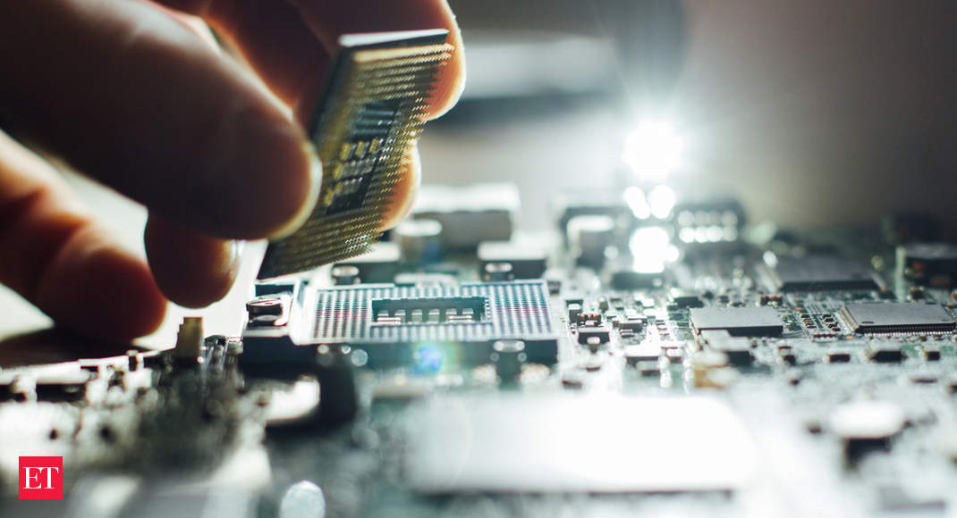
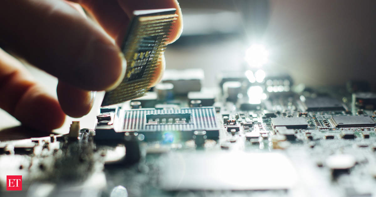
India’s Big Push For Small Chips: Union Government Invites Companies To Submit EoI By Jan 21 For Setting up Semiconductor Fabrication (FAB) Plants In India


In a move aimed at incentivising and attracting investment for setting up of chip manufacturing in India, the Union Ministry of Electronics and Information Technology (MeitY) today issued an notice inviting Expression of Interest (EoI) for setting up / expansion of existing Semiconductor wafer / device fabrication (FAB) facilities in India or acquisition of Semiconductor FABs outside India.

The last date for submission of EoI proposal is Jan 31, 2020.

MeitY asked the interested firm to can indicate the kind of financial support desired from the Government of India, including Grant-in-Aid (GIA), Viability Gap Funding (VGF) in the form of Equity and / or Long-Term Interest Free Loan (LIFL), tax incentives, infrastructure support, etc.
 

shade

Senior Member
Joined
Feb 28, 2016
Messages
14,301
Likes
87,020
Country flag

Lobbyist group wants more gibs exclusively for PCB and PCBA manufacture.
Over and above the gibs already for Mobile and Laptop manufacture.
 

Indx TechStyle

Kitty mod
Mod
Joined
Apr 29, 2015
Messages
18,270
Likes
56,146
Country flag
Isro eyeing new chip unit as more firms take to skies.

Isro is looking to build chips with 65-nanometre technology in the new fab.
How India’s trying to indigenise chip fabrication technology.

IIT Mandi is among the few institutions in India working towards indigenisation of a wide spectrum of photoresists .

In 2012, the institute started an initiative for the research and development of futuristic device fabrication technologies with the support of chipmaker Intel which provided $300,000 for developing state-of-art materials for 20 nanometre (nm) node VLSI technologies.

This was demonstrated for resolution of 20 nm under EUV (extreme ultraviolet lithography) at Lawrence Berkeley National Laboratory, USA.

the Semiconductor Laboratory (SCL) in Mohali uses four different types of photoresists that are sensitive to deep ultraviolet (DUV) light. As no Indian manufacturer develops these DUV resists, SCL is fully dependent on foreign vendors. The IIT Mandi photoresists team is working on developing such DUV resists.

The Space Application Centre (SAC) in Ahmedabad has done some work on 70 nm technology at the R&D level.
 

LondonParisTokyo

Senior Member
Joined
Oct 15, 2015
Messages
2,955
Likes
8,205
Country flag

Lobbyist group wants more gibs exclusively for PCB and PCBA manufacture.
Over and above the gibs already for Mobile and Laptop manufacture.
I hope they get it. Making chips in-house will seriously have the biggest impact on a domestic manufacturing ecosystem.
 

warriorextreme

Senior Member
Joined
Sep 29, 2010
Messages
1,867
Likes
3,040
Country flag

India’s space agency plans to build an additional fab at Semiconductor Laboratory (SCL), its chip making facility in Chandigarh, in a bid to scale up capacity to meet the growing demand for chipsets for rockets and satellites as it opens up the space sector to private firms and startups.

The move by the Indian Space Research Organisation (Isro) comes at a time when the government is looking to encourage global companies to set up semiconductor fabs to tap the local market.

SCL has a 180-nanometre facility that produces chips for strategic purposes. SCL and the Semiconductor Technology and Applied Research Centre (SITAR) in Bengaluru, which has a 100-nanometre unit, also make micro-electrical mechanical systems (MeMs) and sensors that have applications in critical areas. SITAR also runs a Gallium Arsenide Enabling Technology Centre (GAETEC) in Hyderabad.

However, most of the country’s requirement is met by imports due to a lack of a homegrown ecosystem of semiconductor manufacturers.
 

RoaringTigerHiddenDragon

Senior Member
Joined
Sep 5, 2020
Messages
4,013
Likes
17,094
Country flag

India’s space agency plans to build an additional fab at Semiconductor Laboratory (SCL), its chip making facility in Chandigarh, in a bid to scale up capacity to meet the growing demand for chipsets for rockets and satellites as it opens up the space sector to private firms and startups.

The move by the Indian Space Research Organisation (Isro) comes at a time when the government is looking to encourage global companies to set up semiconductor fabs to tap the local market.

SCL has a 180-nanometre facility that produces chips for strategic purposes. SCL and the Semiconductor Technology and Applied Research Centre (SITAR) in Bengaluru, which has a 100-nanometre unit, also make micro-electrical mechanical systems (MeMs) and sensors that have applications in critical areas. SITAR also runs a Gallium Arsenide Enabling Technology Centre (GAETEC) in Hyderabad.

However, most of the country’s requirement is met by imports due to a lack of a homegrown ecosystem of semiconductor manufacturers.
State-of-the-art chip size is 7nm wafers and below during current times. You can see below the MOSFET scale of targeted chip sizes until 2023.


I see numbers like 100nm and 130nm in the replies by members here. Those are 2001-2003, which would imply we are 20 years behind the leaders. Not good.
Is the government looking at players to setup fabs for contemporary 7nm and below or some historic sizes?
 

warriorextreme

Senior Member
Joined
Sep 29, 2010
Messages
1,867
Likes
3,040
Country flag
State-of-the-art chip size is 7nm wafers and below during current times. You can see below the MOSFET scale of targeted chip sizes until 2023.


I see numbers like 100nm and 130nm in the replies by members here. Those are 2001-2003, which would imply we are 20 years behind the leaders. Not good.
Is the government looking at players to setup fabs for contemporary 7nm and below or some historic sizes?
Directly having a fab that can churn out 7nm for us seems very hard to achieve as it will require humungous capital. Government is aiming for 28nm or lower as per below report. If everything works out then we might catchup in next few decades.


SKC

Senior Member
Joined
Aug 16, 2014
Messages
8,785
Likes
30,253
Country flag
State-of-the-art chip size is 7nm wafers and below during current times. You can see below the MOSFET scale of targeted chip sizes until 2023.


I see numbers like 100nm and 130nm in the replies by members here. Those are 2001-2003, which would imply we are 20 years behind the leaders. Not good.
Is the government looking at players to setup fabs for contemporary 7nm and below or some historic sizes?
Dude Chill!
You don't directly make <10 nm fab plants. Only if you have existing setup of higher nodes then you scale down gen by gen.
Also <10nm nodes are for phones and PCs. You don't need such small node for everyday electronics at home. Certainly not for defense and space use. Both defense and space sector use high strength radiation hardened chips often in range of 140-200 nm techniques.
 

RoaringTigerHiddenDragon

Senior Member
Joined
Sep 5, 2020
Messages
4,013
Likes
17,094
Country flag
Dude Chill!
You don't directly make <10 nm fab plants. Only if you have existing setup of higher nodes then you scale down gen by gen.
Also <10nm nodes are for phones and PCs. You don't need such small node for everyday electronics at home. Certainly not for defense and space use. Both defense and space sector use high strength radiation hardened chips often in range of 140-200 nm techniques.
So GoI is inviting fabs for making small volume defence chips? I thought we already had those in places like Chandigarh.
also, no one is asking we go to less than 10nm right away. Targeting 28nm , as #warriorextreme pointed out, which is a 10 years old technology is a decent start.
Also, Even if we don’t have a fab to manufacture 10nm and below chips, we can always R&D and design it to make it in someone else’s fab. You are conflating manufacturing with R&D to get to 10nm and below.
‘Volumes are in phones and other PDAs. No fab is going to be successful without economies of scale and you have to setup fabs that cost billions of dollars in investments. That is only for sensors, pda, laptop world.
 

SKC

Senior Member
Joined
Aug 16, 2014
Messages
8,785
Likes
30,253
Country flag
So GoI is inviting fabs for making small volume defence chips? I thought we already had those in places like Chandigarh.
also, no one is asking we go to less than 10nm right away. Targeting 28nm , as #warriorextreme pointed out, which is a 10 years old technology is a decent start.
Also, Even if we don’t have a fab to manufacture 10nm and below chips, we can always R&D and design it to make it in someone else’s fab. You are conflating manufacturing with R&D to get to 10nm and below.
‘Volumes are in phones and other PDAs. No fab is going to be successful without economies of scale and you have to setup fabs that cost billions of dollars in investments. That is only for sensors, pda, laptop world.
The govt is doing this only. Only you seems to be forcing on getting latest fab nodes directly.
Let companies start with the process which can be started quicker with lower investment. Then they will eventually jump over nodes to closer to global standards.
 

warriorextreme

Senior Member
Joined
Sep 29, 2010
Messages
1,867
Likes
3,040
Country flag
For anyone who wants to understand more about challenges that India faces and the opportunities that Indiah as in terms of semiconductors I would suggest reading all the articles by Mr. Arun Mampazhy.


shade

Senior Member
Joined
Feb 28, 2016
Messages
14,301
Likes
87,020
Country flag
So GoI is inviting fabs for making small volume defence chips? I thought we already had those in places like Chandigarh.
also, no one is asking we go to less than 10nm right away. Targeting 28nm , as #warriorextreme pointed out, which is a 10 years old technology is a decent start.
Also, Even if we don’t have a fab to manufacture 10nm and below chips, we can always R&D and design it to make it in someone else’s fab. You are conflating manufacturing with R&D to get to 10nm and below.
‘Volumes are in phones and other PDAs. No fab is going to be successful without economies of scale and you have to setup fabs that cost billions of dollars in investments. That is only for sensors, pda, laptop world.
You do realize there are a whole lot more types of ICs than the top of the line ARM A series and x86 processors used in Mobiles/Computers right? 28nm should be enough for those.

Going directly for 10nm, 7nm, 5nm is a pain as the equipment for these feature sizes is already "booked" from the vendors like the big wigs like Samsung, TSMC, Intel, Global Foundries( AMD ) etc.
Gormint or even private corps wanting to purchase such machines will be put on the end of the queue and get their orders 3-5 years later.

Then there is the question of availability of big brained engineers to make 10nm and lower possible.

Intel has been struggling to get to 7nm while GF, TSMC and Samsung already have, so clearly equipment is not the only issue.

Machines for 28nm is readily available in second hand form, for cheap( relatively, still goes into crores ).
Perhaps engineering talent wise also engineers can be trained since this is a "mature" technology.

Gormint already has some "scheme" in place to promote Fabless IC design by Indian companies as you have mentioned.

IC fabrication is basically to the Electronics engineering field like what Jet engine manufacturing is to mechanical engineering/materials science.
You want top end right at the start, you have to pay top dollar, and even then success and world beating manufacturing is still not guaranteed, look at China.


Regardless I doubt that after the IC Fab KLPDs from 2014 onwards any private company has any appetite for IC Fabs, so probably Gormint won't find any takers for this scheme.
 

sorcerer

Senior Member
Joined
Apr 13, 2013
Messages
26,919
Likes
98,470
Country flag
India may finally be getting its chip fabrication act together - Latest News | Gadgets Now


India is once again trying to deal with this threat. The government in December called for expressions of interest (EoI) for setting up or expanding existing semiconductor wafer and device fabrication (fab) facilities in the country, or even acquisition of semiconductor fabs outside India.

“The EoI shows we are really serious now,” V K Saraswat, member of the Niti Aayog, said at a webinar organised last week by Times Techies, together with the India Electronics & Semiconductor Association (IESA).


sorcerer

Senior Member
Joined
Apr 13, 2013
Messages
26,919
Likes
98,470
Country flag
Chipmakers Said to Get Over $1 Billion for Setting Up Plants in India


India is offering more than $1 billion (roughly Rs. 7,340 crores) in cash to each semiconductor company that sets up manufacturing units in the country as it seeks to build on its smartphone assembly industry and strengthen its electronics supply chain, two officials said.

Prime Minister Narendra Modi's 'Make in India' drive has helped to turn India into the world's second-biggest mobile manufacturer after China. New Delhi believes it is time for chip companies to set up in the country.


HariPrasad-1

Senior Member
Joined
Jan 7, 2016
Messages
9,598
Likes
21,066
Country flag
Chipmakers Said to Get Over $1 Billion for Setting Up Plants in India


India is offering more than $1 billion (roughly Rs. 7,340 crores) in cash to each semiconductor company that sets up manufacturing units in the country as it seeks to build on its smartphone assembly industry and strengthen its electronics supply chain, two officials said.

Prime Minister Narendra Modi's 'Make in India' drive has helped to turn India into the world's second-biggest mobile manufacturer after China. New Delhi believes it is time for chip companies to set up in the country.

This is going to be a master stroke. This is a big market with little presence of India. We should dominate this. Our visionless politicians ignored this for years.
 

Latest Replies

Global Defence

New threads

Articles

Top